


Development of a TOF Sensor for Long-Range and Stable Wide-Angle Detection
- TOF Laser Sensor
- dTOF
- High-speed laser driver circuit
- APD individual variation correction
- APD temperature compensation
In modern manufacturing, labor shortages due to population decline have increased the need for further automation. Additionally, to respond to diversifying needs and rapid technological innovation, highly flexible automated production is essential. This requires sensors that can reliably detect objects from long distances without obstructing the movement paths or working ranges of equipment and robots. In this study, we focused on a photoelectric sensor using Time-of-Flight (TOF) technology, aiming to achieve stable detection of objects with various colors and surface conditions, such as white or black, rough or glossy, at distances up to 6 meters and within an angular range of ±85°. For particularly challenging targets, such as black-painted automobile bodies, the design target was set at a detection distance of 3.5 meters and an angular range of ±50°. To achieve this, we enhanced the signal-to-noise ratio (S/N ratio) through short-pulse laser diode driving and ultra-high-sensitivity stable operation of an avalanche photodiode (APD), significantly improving detection performance. As a result, even in cases where conventional sensors are limited to ±6° at a distance of 3.5 meters, our technology enables stable detection across a much wider angle of ±66°. Through this advancement, we successfully developed the E3AS-HF TOF laser sensor, which provides high detection stability regardless of object color or surface condition.
1. Introduction
Today, flexible, automated production is a requirement for manufacturers to address diverse market demands and to adapt to rapid technological innovation. In addition, the severe global labor shortage and the COVID-19 pandemic have made it more apparent than ever that manufacturers bear social responsibility to ensure supply availability. Manufacturers are accordingly expected to redouble their automation efforts.
Such automated production requires the effective use of robots and sophisticated automated equipment. Also required are high-precision sensors. These sensors must mount flexibly anywhere and reliably detect the presence or absence of production target objects at a distance without interfering with the motion path or operating range of production equipment. In general, highly directional optical sensors are better suited to detecting the presence or absence of target objects without interfering with the operation of nearby robots or other equipment than ultrasonic or electromagnetic sensors.
Conventional types of photoelectric sensors include transmissive, retroreflective, diffuse-reflective, and other light-quantity detection types, as well as triangulation-based distance-setting types. Each type has constraints and limitations regarding ease of installation and detection performance. For example, transmissive and retroreflective types can detect objects at a distance. However, installing sensor or mirror on both sides of the detection target constrains the layout of the manufacturing equipment. Diffuse reflective sensors are highly susceptible to installation conditions, including the color, surface condition, and mounting angle of the detection target and, therefore, have difficulty achieving reliable detection. Triangulation-based sensors have the advantage of low color susceptibility. However, their practical detection reach is generally limited to approximately 0.5 m. This limitation is due to their large enclosure, which is unavoidable because the light projection and reception units must be sufficiently spaced to achieve a long detection range. As a result, the practically acceptable enclosure size reduces the upper limit of the detection reach.
On the other hand, recent advancements in semiconductor technology have lowered the technological barriers to overcoming the limitations of conventional photoelectric sensors. More specifically, miniaturized semiconductor processes have increased the maximum achievable signal-processing speed and have improved the performance of light-emitting and receiving elements. These advancements have brought ToF-based distance-setting types to a practically feasible level. The ToF system operates on the principle of measuring time and converting it to distance. It is not only more resistant to the color or surface condition of the target object but is also less susceptible to the sensor’s installation state than other alternatives. In addition, it can avoid increasing the enclosure size, thereby enabling long-range detection. However, sensitivity constraints have prevented reliable long-range photoelectric sensors from becoming a reality. Consequently, demand has intensified for a significant increase in the ToF system’s sensitivity.
Against this background, we developed a ToF laser sensor with a long linear range of up to 6 m and a wide angular range of ±85°, which provides enhanced sensitivity and enables the detection of target objects of various colors and surface conditions without interfering with robot operation. The sensor was designed to achieve a target-detection angular range of ±50°. The design premise assumes use in detecting black-coated automotive bodies, which are particularly challenging to detect, at a practically sufficient detection distance of 3.5 m, reflecting the installation location in the production line.
2. ToF laser sensor
2.1 Operating principle of ToF
ToF systems are largely divided into two types by operating principle: direct ToF (dToF) and indirect ToF (iToF).
The iToF system intensity-modulates a laser beam with a specific frequency and uses the resulting phase information to measure the distance to the target object. As shown in Fig. 1, a sine wave or similar continuous wave intensity-modulated at a constant frequency is projected to obtain the phase difference to the reflected light from the target object.
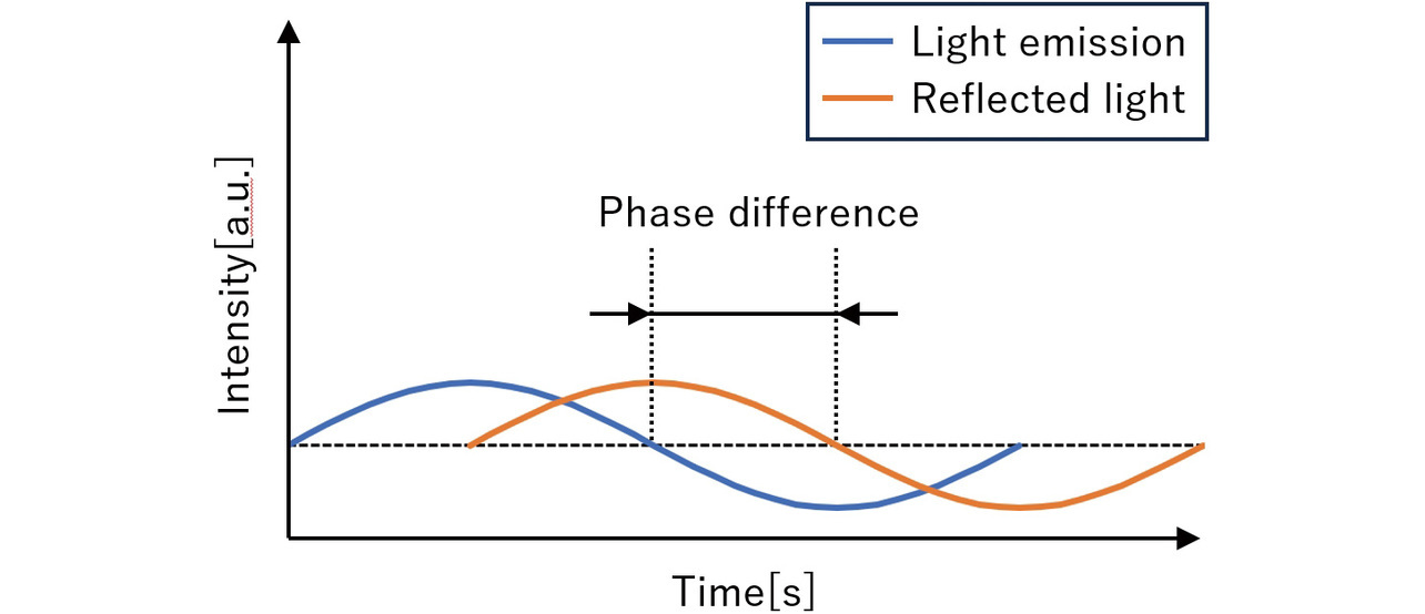
From the phase difference, the distance d is derived using Eq. (1) below:
where c is the light speed (m/s), θ is the phase difference (rad), and f is the modulation wave frequency (Hz). Characteristically, this system generally uses a relatively low modulation frequency, ranging from several megahertz (MHz) to several tens of megahertz, and requires no high system speed, enabling compact size and power savings. An increased frequency would increase the phase resolution, resulting in a sensor with higher detection accuracy. However, from Eq. (1), the required frequency for a detection reach of up to 6 m is 25 MHz or less. In other words, the minimum required light-projection time per distance measurement is at least 40 ns. The Laser Class Standards specify and limit the light output per unit time based on its potential risk to human health, making higher light output unavailable. Thus, the inability to balance range expansion and sensitivity enhancement is a shortcoming of iToF.
On the other hand, the dToF system projects light and directly measures the round-trip time of the light. The round-trip delay time until the projected pulse light bounces back from the target object is measured as shown in Fig. 2.
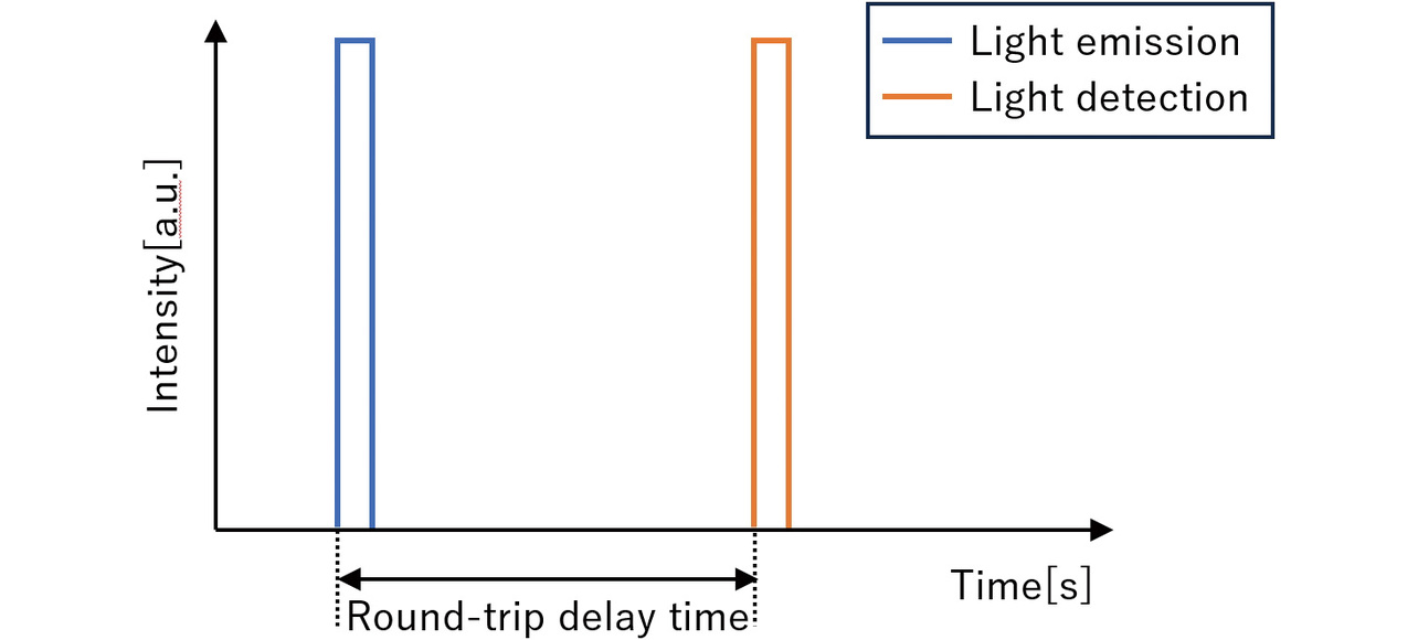
From the round-trip delay time, the distance d is derived using Eq. (2) below:
where c is the light speed (m/s), and Δt is the round-trip delay time from the projection of the pulse light until its return. In theory, dToF enables measuring even ultra-short-pulse light projected on the order of several nanoseconds or less, as long as the light’s frequency falls within the range that the receiver circuit can transmit. Hence, dToF is more convenient than iToF for increasing the light projection power to enhance sensitivity.
From the above, dToF is better suited to long-range detection and high sensitivity, enabling reliable detection of black-coated automotive bodies.
2.2 Challenge to dToF
A system-wide sensitivity improvement is indispensable to ensure reliable dToF detection of black-coated automotive bodies at angles of 50° or more. We set the design target sensitivity based on signal-to-noise ratio (SNR) estimates that reflect the angular reflectance characteristics of automotive bodies and individual variations in sensor components. For the light projection system, we assumed a peak optical output of 500 mW or more. We required a light reception system sensitive enough to detect faint reflected light from a target object. Hence, we set the target at approximately a 50-fold increase in sensitivity over conventional non-amplified photodetectors. This target assumes approximately two- and 50-fold enhancements for the light projection and reception systems, respectively, relative to competing products, yielding an approximately 100-fold sensitivity enhancement.
The light projection system includes a highly directional, linear semiconductor laser diode (LD) for long-range detection, which requires safety considerations. For instance, the Japanese Industrial Standards, JIS C 6802, classify laser diodes into eight-level classes based on the risk level of laser products. Among these classes, Class 1 is considered the safest. Actual manufacturing sites often have laser sensor-mounted equipment close to operators performing assembly or adjustment tasks. Demand is high for Class 1 compliant sensors that can be used without special safety measures. Based on these shop-floor needs and safety requirements, we had to develop an LD drive circuit that maximizes the S/N ratio, a sensor performance indicator, while meeting Class 1 safety standards.
Among the laser class restrictions, the requirements on average optical output power are particularly likely to constrain the design. For the adopted light source wavelength of 660 nm, the average optical output power is below 390 μW. One method to reduce the average optical output power is to extend the LD-projected light pulse cycle. However, this method reduces the number of received signals captured per unit time. As a result, averaging is only partially effective at noise reduction. Therefore, under the condition of not extending the LD-projected light pulse cycle, we decided to meet the average optical output power restrictions by reducing the projected light pulse width to 2.0–3.0 ns, which the receiver circuit can detect. Incidentally, the requirements on single-pulse energy specify that it be below 200 nJ. In addition, LD elements individually vary in luminous efficiency. Hence, the LD drive circuit must have a variable light output capability to correct individual variations and achieve the maximum light output within the constraints. Conventional LD drive circuits control the light output using feedback from the monitor current of the photodiode (PD) contained in the LD package. However, these circuits cannot follow nanosecond-order short pulses. Thus, the challenge for our LD drive circuit is to support a variable light output capability for short-pulse driving.
For the receiver circuit, the most influential factor on the S/N ratio is the selection of the light-receiving element. Table 1 compares the characteristics of a PIN photodiode (PIN PD), APD, and single-photon avalanche diode (SPAD) as representative light-receiving elements1,2). The relative sensitivity row shows relative values to the PIN PD’s light-receiving sensitivity used as the reference value 1.
| Comparative parameter | PIN PD | APD | SPAD |
|---|---|---|---|
| Relative sensitivity* | 1 | 10–100 | ≥ 10,000 |
| Individual variation in breakdown voltage | — | ±10-odd % | ±10-odd % |
| Sensitivity temperature characteristics | None | Several %/°C | Several %/°C |
| Illuminance tolerance | Several ten thousand lx | ≥ 100,000 lx | None |
The PIN PD remains highly stable against temperature changes. However, its relative sensitivity is lower by two or more orders of magnitude than that of the other light-receiving elements. Meanwhile, the SPAD has the highest relative sensitivity. However, in theory, it saturates when responding to a single photon and lacks illuminance tolerance.
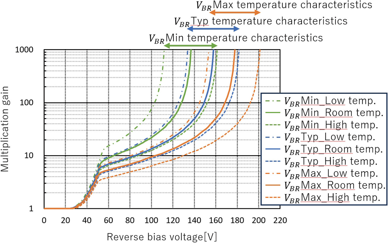
Setting a high multiplication factor using the APD improves the S/N ratio while avoiding the theoretical constraints on sensitivity and illuminance tolerance. This approach enables achieving a 50-fold increase in sensitivity relative to PIN PD. However, the APD has drawbacks, including large individual variations and strong temperature dependence. More specifically, when subjected to a backward voltage, as typically shown in Fig. 3, the APD exhibits pronounced variation in breakdown voltage (VBR). When a threshold voltage is exceeded, the insulation breaks down, allowing a large current to flow. The three sets of color-coded solid, broken, and single-dot chain-line curves represent individual variations in VBR with a maximum-to-minimum difference of approximately 40 V. Moreover, VBR varies significantly because of temperature changes. Each set of curves of the same color indicates the temperature characteristics of VBR. An approximately 50 V difference exists between the maximum and minimum temperatures. Thus, the APD varies significantly in characteristics because of individual variations and temperature fluctuations. Driving the APD at a constant reverse-bias voltage results in variation in the obtained multiplication factor, leading to a loss of stable sensitivity. Therefore, the primary challenge to improving the S/N ratio in the receiver circuit lies in how to establish reverse-bias voltage control to reduce these variation factors while maintaining a high multiplication factor.
3. Technical solution to the challenge
To solve the problem presented in Section 2, we newly designed a short-pulse LD drive circuit to improve the S/N ratio and a reverse-bias voltage control circuit for ultra-high-sensitivity, stable operation of the APD.
3.1 Short-pulse driving of the LD
The enablers for maximizing the S/N ratio while meeting Laser Class 1 limits are short-pulse driving and variable light output capabilities. This subsection considers an LD drive circuit that meets these requirements.
Generally, the Automatic Power Control (APC) system is used to drive LDs. This system detects light output using the monitor current from the photodiode (PD) in the LD package and feedback-controls the forward current to maintain constant output. This system advantageously ensures a stable LD light output despite variations in luminous efficiency caused by temperature changes. However, its restricted response speed is unsuitable for dToF, which requires pulse light emission on the order of nanoseconds. To address this issue, a pulse-driven LD system was proposed that stores and uses a single pulse’s worth of energy in a capacitor or an inductor3). Based on this method, we developed a ToF sensor with a variable light output capability. Fig. 4 shows the configuration of the LD drive circuit.
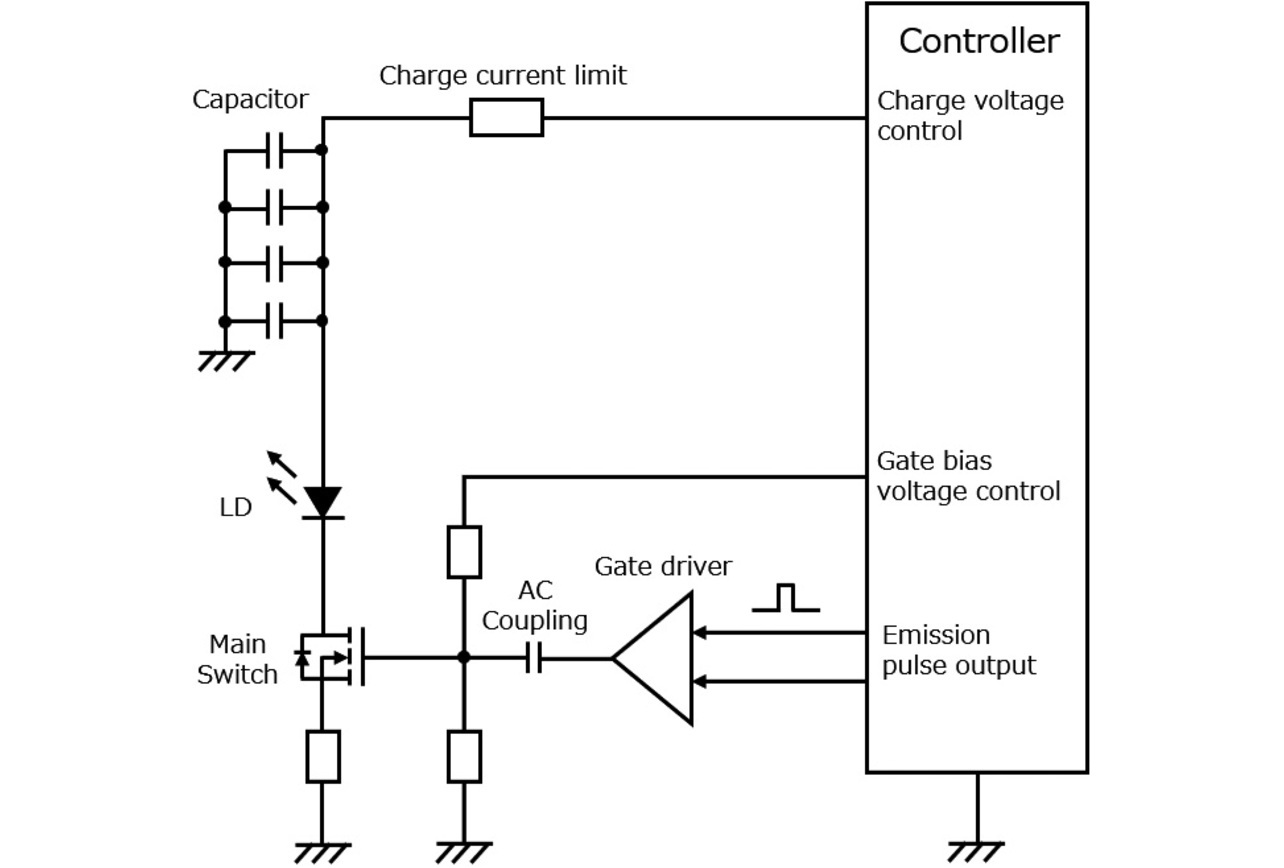
The variable light output capability is provided by the controller, which controls the charging voltage of the capacitor. This control method enables adjusting the variations in the LD and drive circuit during assembly, ensuring a safe maximum power output. Moreover, a user-adjustment function is provided to allow the user to manually adjust the light output. Assume, for example, that the detection target is a mirror or a similar highly reflective object. Using the user adjustment function, the user can reduce light output and prevent oversaturation of the APD, thereby improving detection accuracy. The adopted main switch is a gallium nitride field-effect transistor (GaN FET). GaN FETs offer higher switching speeds, smaller footprints, and higher efficiency than conventional Si MOSFETs. They are already applied to electric vehicles (EVs) and compact USB PD chargers. The combined result of the elements described above in this subsection is our large-current, short-pulse LD driving.
3.2 Ultra-high-sensitivity stable operation of the APD
To correct individual variations in the APD and stabilize its temperature characteristics, we developed an in-process method to estimate each individual’s multiplication factor and a reverse-bias-voltage control circuit to correct it within the sensor.
The three representative methods for estimating the multiplication factor are the photocurrent method, the noise method, and the dark-current/breakdown-voltage method4-6).
The photocurrent method irradiates a device with a given number of photons and measures the resulting photocurrent to calculate the multiplication factor. This method directly measures the current value and yields high accuracy. However, it is prone to instability due to fluctuations in light-source intensity and misalignment, which pose challenges for mass production.
The noise method uses a theoretical formula to calculate the multiplication factor from the APD’s noise current level. This method calculates the multiplication factor from a light-induced mean current and a noise factor, does not require the absolute value of light intensity, and is insensitive to light-source stability. On the other hand, it requires separating measurement-circuit noise from external noise, which can easily complicate the measurement system.
Given the points above, we adopted the dark-current/breakdown-voltage method, which measures the dark current and calculates the breakdown voltage to estimate the multiplication factor from the APD’s multiplication factor vs. reverse-bias voltage curves. This method can be configured in a simple form to shield the APD from light during production, enabling efficient estimation of the multiplication factor and stable mass production while keeping capital costs low.
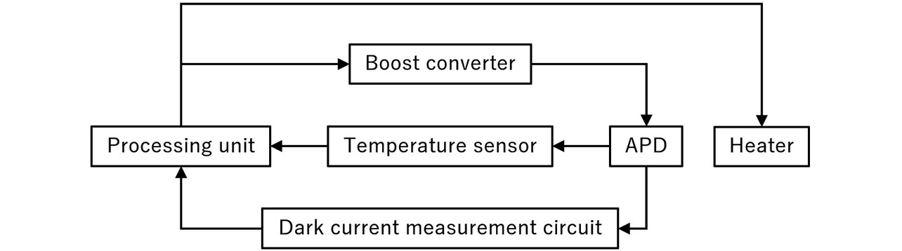
Fig. 5 shows the receiver circuit configuration adopted for multiplication factor estimation and reverse-bias voltage control. A temperature sensor, a heater, a dark-current measurement circuit, and a boost converter are mounted on the sensor’s internal board to enable estimation of the multiplication factor and control of reverse-bias voltage.
Using this circuit, we present below the procedure for determining and controlling the multiplication factor:
During sensor assembly, the reverse-bias voltage applied to the APD is increased stepwise via the boost converter to increase the multiplication factor. Then, when a given voltage threshold is reached, the dark current sharply increases with an increasing multiplication factor as typically shown in Fig. 6. The dark-current measurement circuit monitors this current to record VBR, the boost converter’s output voltage at which it reaches 100 μA. At the same time, the temperature sensor measures and records the temperature at that point. This series of measurements is performed multiple times at different temperatures with the temperature stepwise adjusted using the sensor’s internal heater. The heater is primarily mounted to warm the LD during low-temperature periods. Its use during assembly is designed to rapidly generate a temperature difference, enabling rapid collection of the APD’s individual values.
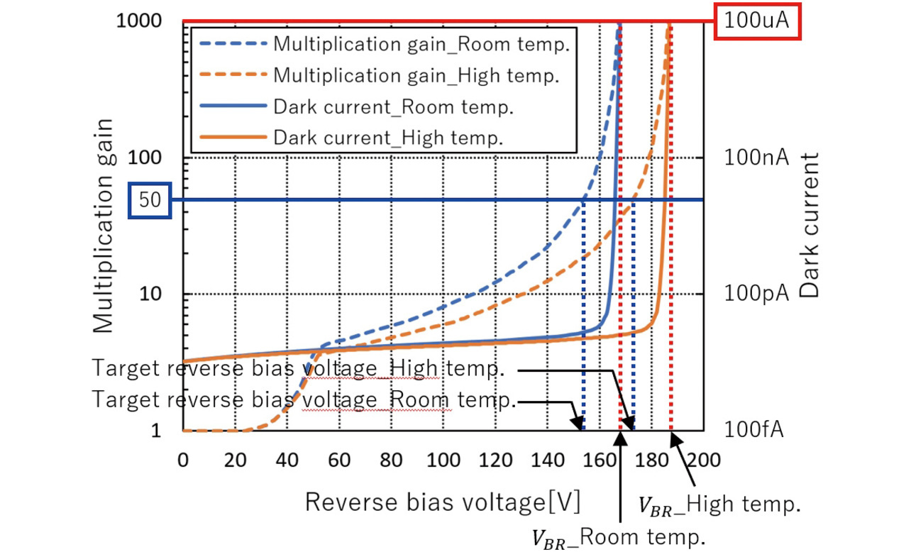
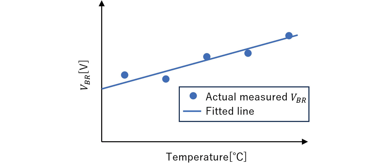
Next, based on the VBR values obtained at each temperature using the aforementioned method, APD’s representative multiplication factor vs. reverse-bias voltage curves are referenced to determine the reverse-bias voltage to obtain the intended multiplication factor. As typically shown in Fig. 7, the calculation results indicate that VBR increases approximately in proportion to the temperature rise. This characteristic is approximated by a linear equation with its slope defined as the temperature coefficient γ, enabling stable multiplication-factor control via temperature-responsive reverse-bias voltage control and reliably yielding high sensitivity.
4. Evaluation experiment
4.1 Performance evaluation of the short-pulse LD drive circuit
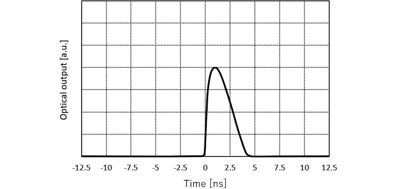
We evaluated our designed LD drive circuit for the LD’s optical pulse shape and variable-light-output operation. The optical pulse shape was measured using an OE converter (Graviton, model SPD-1_650 nm, bandwidth 1.2 GHz) and an oscilloscope (Tektronix, model DPO7354C, bandwidth 3.5 GHz). Fig. 8 shows the optical pulse shape. The optical pulse was well-shaped with no overshoot occurrences observed.
For variable-light-output operation, measurements were performed using an optical power meter (Ophir Optronics Solutions, Model PD300). Incidentally, the PD300 measures only the average optical output power. To calculate the peak optical output, determine the light projection duty cycle from the OE converter’s full width at half-maximum and light projection cycle readings. Then, divide the average optical output power by the duty cycle.
Fig. 9 shows the change in average optical output power as a function of variable capacitor voltage. It confirms that the available light output is almost proportional to the voltage in the region where the capacitor voltage is 3 V or higher. Accordingly, the outgoing product inspection process can correct luminous efficiency variations in LDs, enabling individualized adjustment to maximize light output within Laser Class 1 limits.
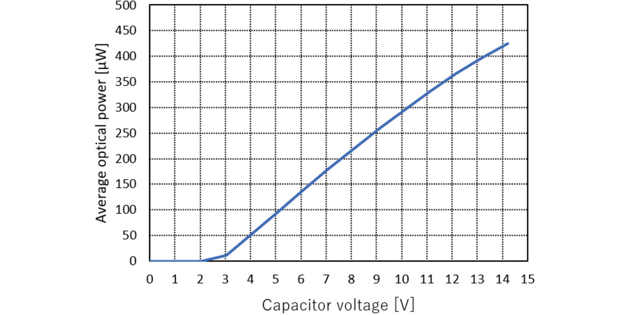
Table 2 sums up the measurement results above. This table confirms the compatibility between short-pulse LD driving and variable-light-output control, enabling an LD drive circuit with a maximum power output within Laser Class 1 limits.
| LD emission characteristics | Target | Measured results |
|---|---|---|
| Full width at half maximum | 2.0 to 3.0 ns | 2.7 ns |
| Peak optical output | ≥ 500 mW | 535 mW |
| Average optical output power (*1) | < 390 μW | 358 μW |
| Single-pulse energy (*1) | < 200 nJ | 1.4 nJ |
4.2 Temperature characterization of the APD’s multiplication factor
In accordance with the procedure in Subsection 3.2, VBR was calculated from the dark current measured using the dark-current/breakdown-voltage method to estimate a reverse-bias voltage that yields a design multiplication factor of 50x. Moreover, the reverse-bias voltage was temperature-corrected based on the VBR obtained by stepwise temperature control with the heater and the temperature coefficient (γ), in other words, the slope of the temperature linear equation. The temperature characteristics were evaluated at 5°C increments with a target multiplication factor of 50x across the ambient temperature range from −20°C to 70°C. Fig. 10 compares the changes in the multiplication factor with and without correction.
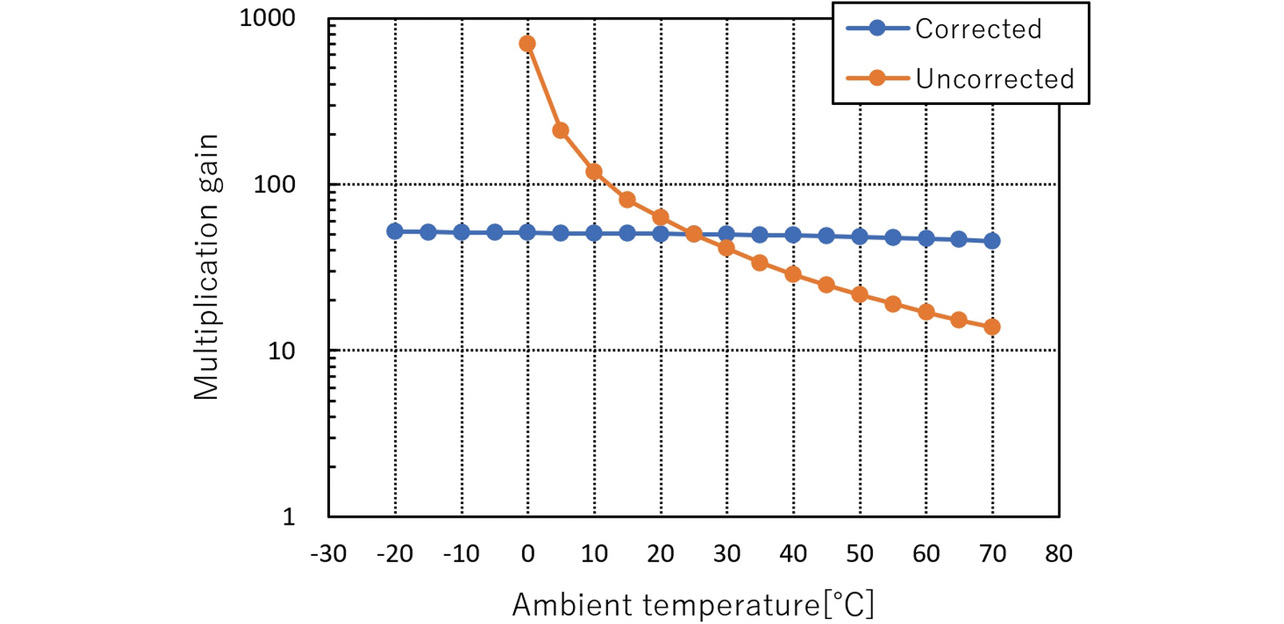
Without correction, the multiplication factor varied significantly from 14x to 700x. However, with correction, the multiplication factor converged to a range of 45.6x to 51.8x around the target value of 50x, which reduced the variation rate to within −9.0% to 3.2%. Thus, the results verify that the APD enables stable driving while maintaining a light-receiving sensitivity approximately 50-fold higher than the conventional 1x sensitivity.
4.3 Evaluation of the detection angular range
The ToF laser sensor developed for a target sensitivity ratio of 100x includes a receiver circuit to correct individual variations in the short-pulse LD drive circuit and the APD. We evaluated it for its detection angular range. For white and black papers with diffuse reflectance, measurements were performed at a detection distance of 6 m with a sensor response speed of 200 ms. As demonstrated in Table 3, the sensor can detect at the measurement system’s maximum controllable angle of ±85° for both white and black papers.
| Comparative parameter | Detection angular range |
|---|---|
| White | ±85° |
| Black paper | ±85° |
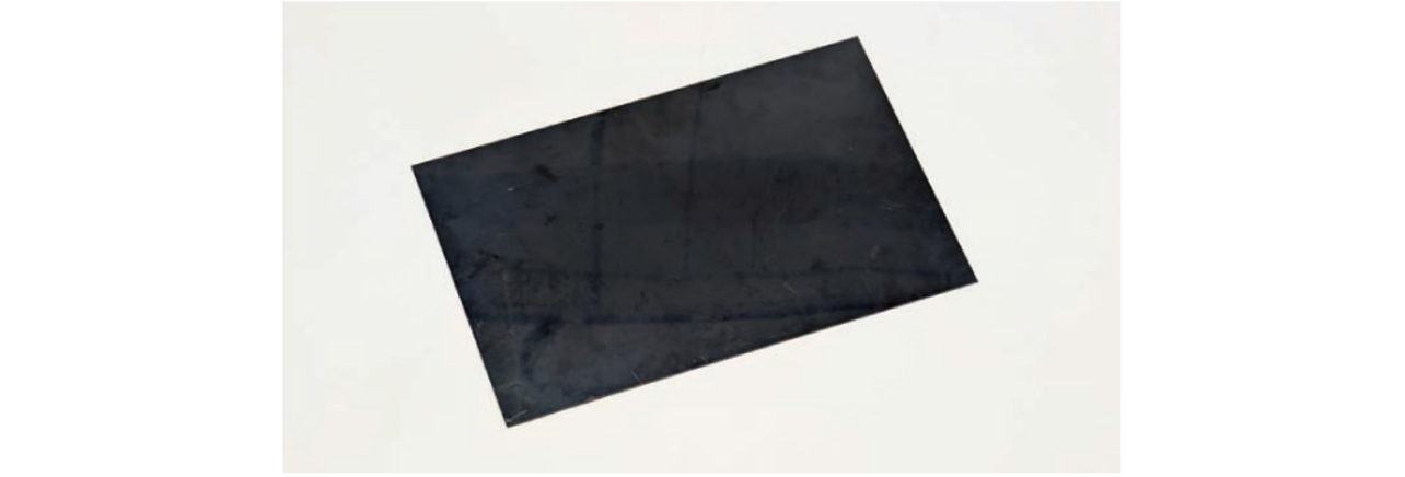
Next, for a black-coated automotive body (Fig. 11) and a black ABS resin (Fig. 12), deemed challenging to detect reliably, measurements were performed at a detection distance of 3.5 m with a sensor response speed of 200 ms. Table 4 shows the results. The evaluation results for a Company A-built sensor are also included for reference. Once the relative angle exceeded ±6° from the black body, the Company A-built sensor failed to detect with its output signal switching from ON to OFF. Meanwhile, our developed sensor demonstrated that it could keep its output signal ON and reliably detect, even angled up to ±66°, well beyond the target value of ±50° and more than 10-fold that of the Company A-built sensor.
| Comparative parameter | Our sensor | Company A-built sensor |
|---|---|---|
| Black body | ±66° | ±6° |
| Black ABS resin | ±75° | ±16° |
As shown above, the short-pulse LD drive circuit and the receiver circuit with APD individual variation correction enable reliable detection with an enhanced S/N ratio, regardless of the target object’s color or surface condition.
5. Conclusions
Our developed sensor is intended to enable advanced automated production. It features long linear and wide angular ranges for reliable detection without interfering with robots’ or equipment’s motion paths or operating ranges, regardless of color or surface condition. Equipped with a short-pulse LD drive circuit and a receiver circuit with APD individual variation correction, this sensor boasts an S/N ratio high enough to detect even black-coated automotive bodies at a relative angle of ±66°.
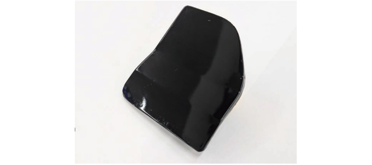
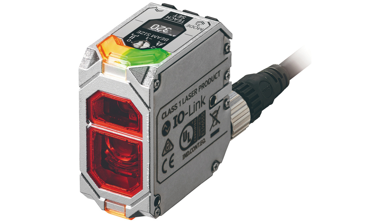
We released a product featuring this technology, the E3AS-HF Series ToF laser sensor (Fig. 13), in March 2025.
Moving on, we will further our technical efforts in sensitivity enhancement and miniaturization and develop easier-to-use sensors to maximize production efficiency for customers.
References
- 1)
- Hamamatsu Photonics. Data sheet/Si APD S14644 Series. (in Japanese), (2021). Accessed: May 27, 2025. [Online]. Available: https://www.hamamatsu.com/content/dam/hamamatsu-photonics/sites/documents/99_SALES_LIBRARY/ssd/s14644_series_kapd1067j.pdf
- 2)
- Hamamatsu Photonics. Data sheet/SPAD (Single Photon Avalanche Diode) S16835 Series. (in Japanese), (2024). Accessed: May 27, 2025. [Online]. Available: https://www.hamamatsu.com/content/dam/hamamatsu-photonics/sites/documents/99_SALES_LIBRARY/ssd/s16835_series_kapd1087j.pdf
- 3)
- Efficient Power Conversion (EPC). AN032 Design of High Current Nanosecond Resonant Pulse Drivers for Laser Diodes, Lidar, and other Applications. (in Japanese), (2024). Accessed: May. 27, 2025. [Online]. Available: https://epc-co.com/epc/Portals/0/epc/documents/application-notes/AN032%20Design%20of%20High%20Current%20Nanosecond%20Resonant%20Pulse%20Drivers-jp.pdf
- 4)
- K. Tsujino et al., “Experimental Determination of the Gain Distribution of an Avalanche Photodiode at Low Gains,” IEEE Electron Device Lett., vol. 30, no. 1, pp. 24– 26, 2009.
- 5)
- Hamamatsu Photonics. Technical documentation/Si APD. (in Japanese), (2025). Accessed: May. 27, 2025. [Online]. Available: https://www.hamamatsu.com/content/dam/hamamatsu-photonics/sites/documents/99_SALES_LIBRARY/ssd/si-apd_kapd9007j.pdf
- 6)
- Japanese Industrial Standards, JIS C 5954-8:2025, 2025.
The names of products in the text may be trademarks of each company.