


High-accuracy Synchronization Technology for PCI Express in Real-Time Systems
- PLC
- Real Time System
- PCI Express
- Time Synchronization
- DMA
In the NJ and NX series of OMRON’s machine automation controllers, the internal central processing unit (CPU) and the internal devices are connected using PCI Express (PCIe). One of the features of PCIe is that it allows direct memory access (DMA) to execute the data transfer without going through the CPU. To introduce PCIe into real-time systems, such as machine automation controllers, it is necessary to control the DMA transfer timing to avoid memory resource conflicts.
Traditionally, centralized control by a single CPU made it easy to control DMA transfer timing and avoid memory resource conflicts. However, modern real-time systems require multifunctionality as well as high-speed and high-precision control cycles. To achieve both, distributed processing architecture is needed where multiple PCIe devices perform DMA transfers with the CPU. To prevent impacts on real-time processing, each PCIe device must transfer data at timings synchronized with the control cycle and with high precision.
This paper proposes a resource conflict avoidance technology for PCIe devices with the CPU and a high-precision time synchronization technology using hardware, which is essential to realize this technology. Synchronization accuracy can be achieved in less than 39 ns. This allows multiple PCIe devices to perform DMA transfers with the CPU while minimizing the impact on real-time processing.
1. Introduction
OMRON-developed NJ and NX Series machine automation controllers1) (hereinafter “controllers”) are real-time systems that enable fast, high-precision control. These controllers perform real-time control processing using high-performance general-purpose central processing units (hereinafter “general-purpose CPU”) to handle complex control processing at high speed. General-purpose CPUs are adopted to enable enhanced real-time processing performance in response to real-world advances in semiconductor technology. However, general-purpose CPUs are not tailor-designed for real-time systems and, as such, rarely include a timer circuit necessary to perform control with a fixed cycle and low delay. Where the intention is to perform processing with low delay, the preferred approach is to generate timer interrupts corresponding to current processing rather than determining which type of processing to perform each time a timer interrupt occurs. To address this issue, multiple timer circuits are required. However, the use of general-purpose CPUs alone does not enable the reliable generation of the multiple timing conditions needed for real-time control.
To address this issue, controllers include a unique built-in timer device (hereinafter “timer device”). Such a timer device contains multiple timer circuits and can generate multiple accurate interrupts at times appropriate to control a real-time system. In response to these interrupts, the general-purpose CPU performs processing, thereby achieving fixed-cycle, low-delay processing.
Typically, for general-purpose CPUs, a broadband general-purpose bus interface known as Peripheral Component Interconnect Express (PCI Express2), hereinafter, “PCIe”) provides a standard bus for the connection to external devices. PCIe is also used in our controllers to connect their general-purpose CPUs and timer devices.
In controllers, general-purpose CPUs are PCIe-connected not only to timer devices but also to interface conversion devices that access field or local buses. For data transfer between a general-purpose CPU and a PCIe device, data transfer occurs between the general-purpose CPU’s memory and the PCIe device through program transfers, where the general-purpose CPU instructs the PCIe device to perform a read or write operation. However, data transfer requires an instruction from the general-purpose CPU, which consumes the CPU’s computational resources, pushing up the transfer overhead.
The common practice to address this challenge is to establish PCIe communication via a function called direct memory access (DMA) transfer, which allows direct device-to-device access to data memory areas bypassing the CPU’s arithmetic processing part. An effective use of DMA transfer enables fast data transfer between the general-purpose CPU’s memory and PCIe devices without imposing arithmetic loads on the general-purpose CPU.
In recent years, demands have increased for controllers featuring non-real-time functions in addition to control processing that requires real-time functionality. Such functions include communication with other devices. The integration of such non-real-time functions into controllers has increased the load on the arithmetic processing of their general-purpose CPUs. The coexistence of real- and non-real-time processing on a single CPU leads to resource contention, which is beginning to affect real-time control performance. Under such circumstances, considerations are underway on distributed architectures for controllers and other real-time systems. In such architectures, non-control processing is performed on a CPU dedicated to non-real-time processing (hereinafter referred to as a “non-real-time CPU”), which does not perform control processing, unlike a control CPU, which is a CPU dedicated to control processing. One form of distributed architecture involves connecting a non-real-time CPU and a control CPU via PCIe to enable data exchange using DMA.
Data transfer from a non-real-time CPU to a control CPU occurs asynchronously with the control cycle. However, the standard PCIe function lacks a mechanism for controlling data-transfer timing. Depending on the timing, data transfer occurs during critical control processing performed by the control CPU. As a result, memory access-related resource contention may occur, which affects control processing. The key to minimizing the impact of data transfer on control processing is to ensure that it does not occur during critical control processing. For this purpose, the timing of control processing and that of the DMA transfer must be synchronized and controlled with high precision.
To achieve this functionality, this paper proposes a data transfer method that combines precise multi-PCIe device time synchronization with DMA transfer timing control.
2. Use of PCIe in real-time systems
2.1 Conventionally configured controller
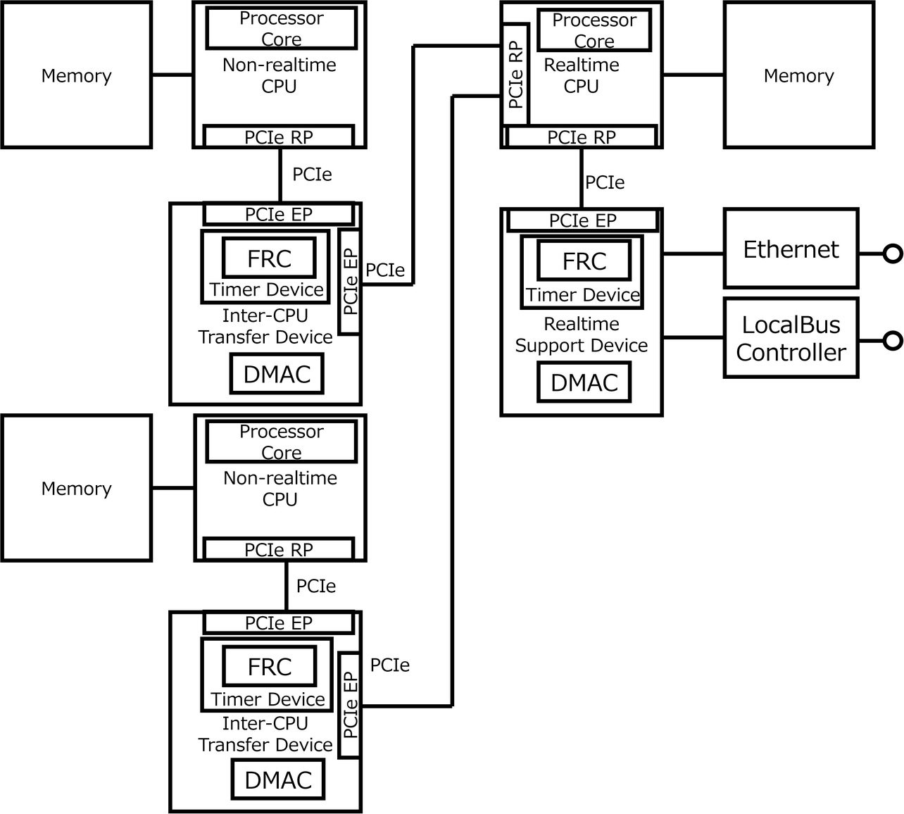
Fig. 1 shows a conventionally configured controller system comprising a device with an interface conversion function and a timer function (hereinafter “real-time support device”) that is required to support a real-time system and a general-purpose CPU for the controller. The general-purpose CPU and the real-time support device are PCIe-connected with a PCIe root port (RP) on the general-purpose CPU side and a PCIe endpoint (EP) on the real-time support device side.
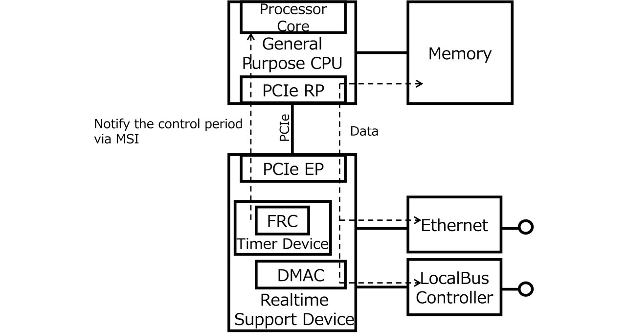
As shown in Fig. 1, the real-time support device includes a built-in timer device. The timer device has an internal counter called a free running counter (FRC). As a source of time information, the FRC continuously counts with high precision at nanosecond (ns) resolution. The timer device notifies the general-purpose CPU of an interrupt using the message signal interrupt (MSI) capability, one of the PCIe’s functions, when the FRC reaches a preset value. The general-purpose CPU receives the interrupt notification and can perform control processing using the interrupt as a starting point.
The timer device can generate interrupts at a constant cycle referencing the high-precision FRC, whereby the general-purpose CPU can perform control processing at a fixed cycle.
Moreover, the real-time support device has in it a DMA controller (DMAC) as a data transfer device to an external interface or a controller’s local bus as shown in Fig. 1. A DMA transfer instruction from the general-purpose CPU to the DMAC via PCIe enables data transfer to the external interfaces (Ethernet and local bus) at times that do not affect control.
2.2 Evolution of controllers into distributed processing systems
In recent years, demand has increased for controllers to be equipped not only with control but also with other functions, such as communication. To address these demands, functions beyond control are being incorporated into controllers. However, add-ons often demand high computing power. Their inclusion is causing problems, such as adverse impacts on control processing.
One way to strike a balance between control performance and add-ons is to evolve controllers and other real-time systems into distributed processing systems that offload add-ons to a non-real-time CPU. Fig. 2 shows a typical connection diagram of general-purpose CPUs in a real-time system for implementing distributed processing. Each non-real-time CPU is PCIe-connected to the control CPU via an inter-CPU transfer device with a built-in DMAC. The single control CPU supports the connection to multiple non-real-time CPUs. Connection to multiple non-real-time CPUs enables the system to expand to match the capacity of the add-ons. Each non-real-time CPU uses the DMAC of the inter-CPU transfer device to perform data exchange with the control CPU. As a result, necessary data transfers can bypass the arithmetic processing part of each CPU without imposing additional computational processing loads on it.
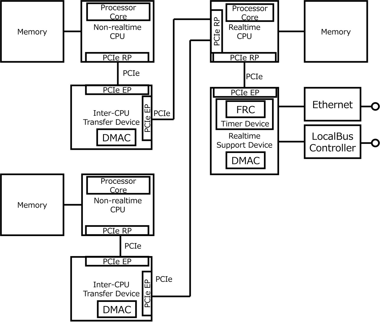
In the configuration shown in Fig. 2, transfer via DMA occurs between each non-real-time CPU’s memory and the control CPU’s memory. The timing of the DMAC’s data transfer execution depends on that of its start-up. The non-real-time CPUs start the DMAC regardless of whether the control CPU is in the middle of real-time processing, which means data transfers occur asynchronously with control processing. The control CPU frequently accesses the memory during real-time processing. Hence, the key to maintaining real-time functionality is to prevent interference with memory access during real-time processing. Memory access via DMA from a non-real-time CPU during real-time processing on the control CPU may cause resource conflicts on the latter CPU. As a result, real-time processing may not complete within the specified time. Moreover, in a system with multiple non-real-time CPUs connected to the control CPU, the volume of data transfer via DMA also increases, further severely affecting the real-time performance of the control CPU.
2.3 Challenge in DMAC configuration for the connection between PCIe RPs
The enabler of DMA transfer instructions to both control-purpose and non-real-time CPUs is the firmware (FW). For a DMA transfer to occur, the transfer-destination memory address is necessary. To fetch this address, the firmware must establish a handshake with the transfer destination. One desirable, simple form of FW-driven DMA transfer control would be to enable transfers between the control and non-real-time CPUs via DMA without requiring a known transfer destination address. An inter-CPU transfer device with DMAC functionality to achieve this purpose would be provided by a configuration3) with a TX-side DMAC and an RX-side DMAC, such as the one shown in Fig. 3. Then, each CPU would control its corresponding RX-side DMAC, which it could specify as the memory address under its control.
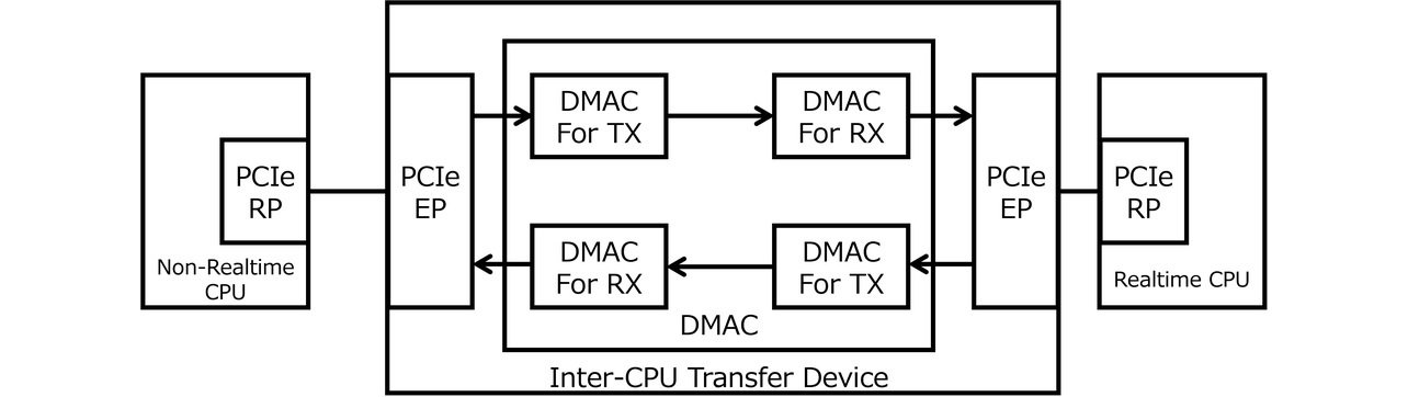
For control processing to occur in a real-time system, all the necessary data must be ready and available. Therefore, the point is that the other side must receive the transmitted data without fail. For this purpose, each CPU starts up its corresponding RX-side DMAC and keeps it ready for reception. As a result, data transmission to the memory area becomes possible without a backlog in the inter-CPU transfer device, ensuring immediate reception on the other side.
For data transfer, each CPU starts up its corresponding TX-side DMAC. Each TX-side DMAC fetches data from its corresponding CPU’s memory and forwards it via the RX-side DMAC to the other end’s memory. Thus, the timing of transmission is determined by each CPU. While in the middle of processing that may affect real-time functionality, the control CPU can avoid starting up the DMAC to inhibit data transmission. On the other hand, regarding reception, the DMAC must remain ready at all times. Hence, there is no stopping incoming data transfers. The timing of incoming data transfers to the control CPU depends on the timing of transmission from the non-real-time CPU-side DMAC. As a result, for instance, the control CPU’s real-time performance may suffer depending on the timing of DMA transfers.
3. Our proposed method and a newly surfaced issue
To resolve the abovementioned DMA transfer timing issue, the DMAC connected to each PCIe interface must perform transfers while avoiding periods of real-time processing on the control CPU. To achieve this purpose, this section proposes a timer function that precisely time-synchronizes with the control CPU and a DMAC-based data transfer method that automatically controls transfer timing based on the timer.
3.1 DMAC transfer timing control
Aiming to minimize the impact on real-time processing, this subsection proposes a DMA transfer mask function4) that automatically pause and resumes data transfer from non-real-time CPUs to the control CPU.
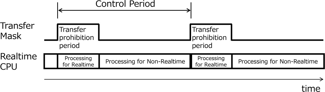
Fig. 4 shows a timing chart for the DMA transfer mask function. This transfer mask function is part of the inter-CPU transfer device. An alternative method uses hardware-generated signals from the real-time support device to trigger mask ON/OFF. However, this alternative method requires adding a mask signal at every increase in the number of inter-CPU transfer devices. Our purpose is to add a transfer mask function flexibly to multiple inter-CPU transfer devices without requiring hardware changes. Hence, we propose a method in which each inter-CPU transfer device generates mask control events. With the transfer mask ON, the inter-CPU transfer device temporarily stop the DMA transfer in progress from the non-real-time CPU to the control CPU. This temporary stop is achieved by prohibiting the transmission of the next PCIe packet to the RX-side DMAC of the inter-CPU transfer device. After the transfer mask is OFF, the DMA transfer resumes. PCIe transfers data in chunks (packets) and cannot stop mid-packet. For our purposes, the PCIe packet size is fixed at a minimum of 128 bytes to ensure an immediate stop of the transfer as a temporary stop is needed and to minimize impact on real-time processing. As a result, the number of packets increases, reducing transfer efficiency and bandwidth. On the other hand, the time from when the transfer mask is ON until the temporary stop of a DMA transfer will be minimized, making it easier to ensure the fixed cyclicity for real-time processing.
Regarding transfer masks, multiple masks can be applied per inter-CPU transfer device. Even with multiple non-real-time CPUs connected to the control CPU, DMA transfer times can be individually specified to help reduce memory contention.
3.2 High-precision time synchronization between PCIe nodes and a newly surfaced issue
The abovementioned DMA transfer mask function is intended to control the temporary stop/resumption of DMA transfers in sync with the moments when the FRC in each inter-CPU transfer device aligns with the mask start and end times set for it by the firmware on the control CPU. In this case, for each control cycle, the control CPU must specify a new mask set value for each inter-CPU transfer device, placing a load on the firmware. To address this issue, our adopted configuration ensures that each inter-CPU transfer device periodically updates the DMA transfer mask function settings. In other words, the controller operates at a fixed cycle and performs the initial cycle and transfer ban period setup for each inter-CPU transfer device via the firmware on the control CPU, ensuring that the DMA transfer mask function is triggered in proper sync with the control cycle. Once the initial setup is complete, FW-driven control is unnecessary, including periodic mask reconfiguration. For this DMA transfer mask function to be triggered synchronously with the control cycle, each inter-CPU transfer device must include a timer device as shown in Fig. 5. This configuration is necessary to ensure precise synchronization of the timer value between the timer device in the real-time support device and that in each inter-CPU transfer device. The required synchronization precision for control between the controller and external equipment is 1 μs or less. The design target for the controller to achieve this synchronization precision is to keep fluctuations in control processing within 10% of 1 μs, in other words, 100 ns.
The key to achieving this target is high-precision time synchronization between the timer devices. Depending on the desired timing of the temporary stop, a DMA transfer continues until up to 128 bytes have been transferred. In other words, the maximum time until the transfer stop is 61 ns, which is equal to the time required to transfer 128 bytes via PCIe Gen1 X1. Because the target precision for inter-equipment synchronization is 100 ns or less, the maximum required time of 61 ns for the temporary stop of the DMA transfer must be factored in. Thus, the target for inter-timer device synchronization is to time-synchronize the timer device time values for the real-time support device and each inter-CPU transfer device with high precision to within 39 ns. High-precision time synchronization between the timer devices can be achieved through precise value synchronization provided by the FRC referenced by each timer.
Each inter-CPU transfer device and the real-time support device use independent reference clocks. Consequently, a phenomenon occurs in which their respective FRCs gradually start to deviate because of the deviation of each reference clock. A clock oscillator used as a reference clock, if relatively precise, would have a deviation of up to approximately ±25 ns/ms. Assume that such oscillators are adopted as the reference clocks for a configuration comprising inter-CPU transfer devices with each equipped with a timer device as shown in Fig. 5. Then, their relative precision to each inter-CPU transfer device side clock may be off by up to ±50 ns/ms, doubled from the abovementioned value. For precise synchronization of the FRC value for each inter-CPU transfer device, their FRC values must be periodically corrected to that of the real-time support device used as the reference. In the conventionally adopted time-synchronization implementation method, the firmware fetched time information from each FRC and periodically corrected the target FRC. For high-precision synchronization of the FRC value, the correction cycle must be short. However, a short correction cycle would increase the control CPU’s computational load, thereby degrading control performance.
As an example, assume a case in which correction is performed once per 8 ms as premised on FW-driven time synchronization. Then, an offset of up to ±400 ns per 8 ms cycle may occur. As mentioned above, the required synchronization precision is 39 ns or less. Hence, a ±400 ns offset in time information poses a serious problem. The next section proposes a high-precision time-synchronization technology to address this problem.
4. Proposal for a solution to the high-precision time synchronization issue
4.1 Hardware-based time synchronization
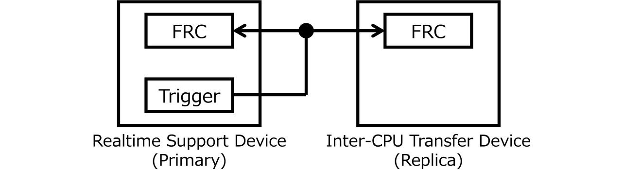
To ensure that the DMA transfer mask function described above is triggered with high precision, the PCIe devices must share the same time information and remain precisely synchronized. This subsection uses Fig. 6 to explain one of the conventional methods adopted for inter-device time synchronization. A trigger signal is transmitted from the device containing the primary FRC. Both the primary and replica FRCs save their current values at the time of trigger signal reception. These saved values are then compared to determine the difference to correct the replica FRC to achieve the intended time synchronization.
The conventional method uses firmware to instruct the primary device to fire a trigger. Next, the firmware fetches the primary and replica FRC values. The replica FRC is corrected based on the differences between the FRC values fetched by the firmware. This method needs to be performed at frequent, periodic cycles, which tends to increase the load on the firmware. To reduce the load on the firmware and accelerate time correction, this subsection proposes developing a hardware-based processing method5).
Fig. 7 shows a configuration diagram for hardware-based time correction. The primary device is configured to fetch the FRC value upon trigger firing and to directly transfer it to the replica devices via asynchronous serial transmission over a single dedicated line, independent of PCIe. Even in a configuration with multiple replica devices, FRC data is transmitted and broadcast from the primary device to all replicas via a multi-drop connection.
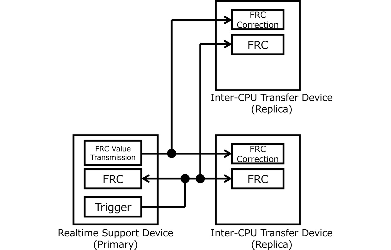
Fig. 8 shows a timing diagram for time correction. First, the primary device fires a trigger. The primary and replica devices save their current FRC values at the time of trigger signal reception. Next, the primary device transmits the FRC value it saved to the replica devices. Each replica device compares the FRC value from the primary device with its own saved value, yielding a difference for which the replica FRC is compensated. This sequence enables an exclusively hardware-based time synchronization implementation without relying on firmware.

5. Effects of our proposed method
This section presents an in situ verification of the hardware-based fast time synchronization proposed in the previous section and shows the obtained results in Figs. 9 and 10.
After time synchronization, the magnitude of the time difference between the primary and replica devices varies depending on the correction. The factor that most strongly affects the magnitude of the difference is the correction cycle. Hence, the in situ verification compared the FRC value outputs at the correction cycles of 8 ms and 250 μs.
Let us outline the correction method adopted for this in situ verification. Examples abound of implementing the replica-side correction for time synchronization. One of the simplest methods is to copy the primary-side FRC value to the replica side as recognized by the latter side. With this method, however, the FRC value may vary significantly, affecting the timer that uses it. Hence, the common practice is to perform correction, such as applying positive or negative offsets to FRC in fine increments/decrements. For this in situ verification, the circuit was designed to perform corrections up to 100 ns. The corrections were applied in increments/decrements of 1 ns/70 μs for the 8 ms correction cycle, and 1 ns/μs for the 250 μs cycle.
5.1 In situ verification of the hardware-based time synchronization method
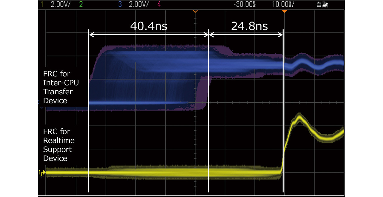
Fig. 9 shows the results of the hardware-based time synchronization proposed in the previous section. Fig. 9 compares the real-time support device-side and inter-CPU transfer device-side FRCs using the oscilloscope waveforms of the selected FRC bits recorded under the configuration shown in Fig. 2. This figure shows the results of observing the waveform for the CPU-side transfer device with the rise of the waveform for the real-time support device side used as the trigger. In Fig. 9, hardware correction was performed once every 8 ms, resulting in an offset ranging from –65.2 to –24.8 ns (median: –45.0 ns) relative to the control CPU-side FRC used as the correction reference. The adopted FRC value correction method incrementally/decrementally adjusted each FRC’s value. As a result, the FRC value correction was completed after an interval following the trigger occurrence. During this interval following the trigger, the FRC value offset present at the trigger occurrence was corrected before completion of the FRC value correction. However, an FRC offset occurred during the period until the correction was completed. The interval following the trigger is inferred to have manifested as the 24.8 ns offset. By the same token, an FRC offset of 40.4 ns likely occurred during the 8 ms between the completion of the first FRC correction and the start of the second FRC correction.
This method demonstrated that time synchronization can be implemented without relying on firmware. For time synchronization at 8 ms cycles, a drift of up to 400 ns could theoretically have occurred. Under relatively favorable experimental conditions, including the use of a high-precision oscillator and ambient temperature, the observed time difference remained small on the approximate order of 65 ns.
5.2 Effects of hardware-based time correction cycle reduction
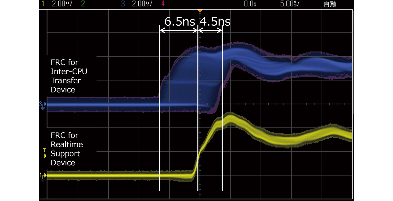
Fig. 10 shows the results of highly frequent time corrections performed to implement hardware-based high-precision time synchronization. The adoption of hardware-based corrections enabled a correction cycle as short as 250 μs. The synchronization precision achieved ranged from –6.5 ns to +4.5 ns (median: –1.0 ns). Thus, the synchronization precision significantly improved compared with the correction at an 8 ms cycle.
Each timer device used in our experiment has an 8 ns clock cycle with the trigger signal latched to the 8 ns clock. The trigger signal and the clock are mutually asynchronous. Hence, a time synchronization error of ±8 ns occurs, depending on the timing of the trigger signal latching. As a result of this error, the inter-CPU transfer devices are likely to have advanced by up to +4.5 ns relative to the real-time support device as observed in Fig. 10.
The in situ evaluation demonstrated that a shorter correction cycle significantly improved the precision of FRC value synchronization, achieving 11 ns, an error well below the target of 39 ns.
This hardware-based time synchronization technology can precisely synchronize the FRC value of the real-time support device with that of each inter-CPU transfer device, enabling the DMA transfer mask function to be triggered with high precision. This technology enables assigning multiple DMA transfer masks to multiple inter-CPU transfer devices on an each basis. As a result, it supports concurrent DMA transfers across multiple inter-CPU transfer devices without memory conflicts and minimizes the impact on the real-time system.
6. Conclusions
This paper discusses technologies necessary to apply PCIe to real-time systems. It presents a distributed real-time system configuration as an evolutionary form of controllers. To address the challenge that DMA transfers from multiple PCIe devices can compromise the real-time performance of distributed real-time systems, we propose a mechanism that inhibits DMA transfers during real-time processing via a DMA transfer mask function. In the course of ensuring the proper triggering of the DMA transfer mask function, a new problem surfaced: the timer values of the timer devices in the real-time support device and each inter-CPU transfer device must be synchronized to align precisely with DMA transfer timing. To address this problem, we propose a new hardware-based time synchronization technology that enables highly frequent synchronization, thereby achieving the target synchronization precision.
In the future, an increasing number of PCIe devices will be used in real-time systems. In particular, controllers employing time-sensitive networking (TSN) and other protocols will be required to maintain real-time connections with external equipment. Time synchronization has become a critical component of controllers used as real-time systems. The precision of internal time synchronization in controllers is also closely related to synchronization with external equipment. The time synchronization technology proposed in this paper will serve as a key enabler for precise time synchronization with external equipment.
References
- 1)
- OMRON Corporation, NJ/NX Series Machine Automation Controllers, AHth Edition (2025), (in Japanese), Accessed: Feb. 17, 2025. [Online]. Available: https://www.fa.omron.co.jp/data_pdf/cat/nj_nx_sbca-100_14_2.pdf
- 2)
- PCI-SIG, PCI Express Base Specification Revision 2.1, 2009.
- 3)
- OMRON Corporation, “TRANSFER APPARATUS, INFORMATION PROCESSING APPARATUS, AND DATA TRANSFER METHOD,” Japanese Patent No. 7326863 (in Japanese), Aug. 7, 2023.
- 4)
- OMRON Corporation, “INFORMATION PROCESSING APPARATUS,” (in Japanese), Japanese Patent No. 7259537, Apr. 10, 2023.
- 5)
- OMRON Corporation, “CONTROL APPARATUS,” (in Japanese), Japanese Unexamined Patent Application Publication No. 2022-119703, Aug. 17, 2022.
The names of products in the text may be trademarks of each company.
PCIe and PCI Express are registered trademarks of PCI-SIG.
Ethernet is a registered trademark of Fuji Film Business Innovation Co., Ltd.