


ASIC (Application Specific Integrated Circuit) Remake Method Guaranteeing Compatibility at the Clock Cycle Level
- ASIC
- End of Life
- Remake
- Asynchronous Circuit
- PLC
In recent years, the domestic semiconductor industry has faced intense competition and supply chain disruptions due to semiconductor shortages. Amid the phaseout of ASIC production using older processes, we have struggled with how to respond when ASIC production is discontinued to maintain product supply to customers. Common responses include bulk purchases (last buys) or redesigns (remakes). However, redesigns often face the challenges of the lack of design assets and technical issues with asynchronous circuits widely used in older ASICs.
To address these challenges, we propose a development method that enables a redesign from asynchronous to synchronous circuits even when design assets are unavailable. Specifically, in RTL verification, we simultaneously input signals to both the original RTL circuit, which is asynchronous, and the RTL redesigned into synchronous circuits. By comparing the output signals from each RTL circuit clock by clock, we overcome these challenges simultaneously, ensuring functional and performance compatibility. We have already remade six ASICs using this method and achieved zero market claims.
1. Introduction
1.1 Trends in the semiconductor industry
Many domestic semiconductor vendors are downsizing and exiting amid the recent intensifying competition with overseas competitors1,2). Moreover, such factors as the COVID-19 pandemic, natural disasters due to floods, earthquakes, and the like, and US-China decoupling and other geopolitical factors have led to the current semiconductor shortage, wreaking massive havoc on the global supply chain. Under these circumstances, some semiconductor vendors, both at home and abroad, are expected to concentrate their resources on cutting-edge processes with high value-added rates3), thereby accelerating the phaseout of obsolete production processes.
1.2 Our preparedness for discontinuation of semiconductor parts
Our CS/CJ Series products contain many semiconductor components called ASICs. An ASIC is a type of semiconductor integrated circuit optimized to suit a specific application or purpose. Optimally designed for a specific function and process, ASICs serve as a means to achieve product performance improvement and differentiation.
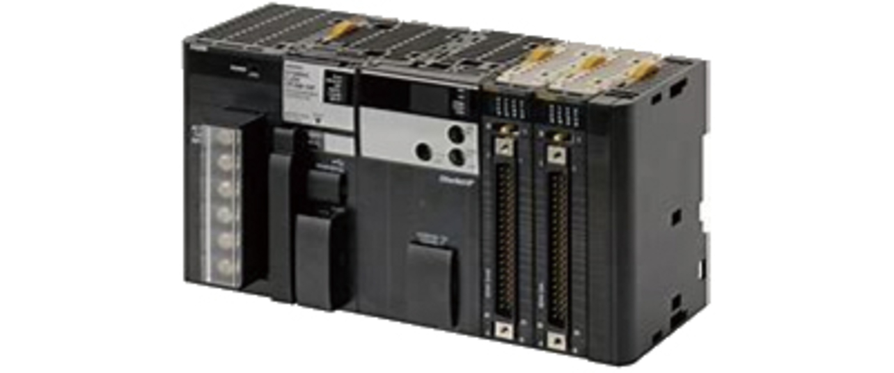
The CS/CJ Series is a lineup of general-purpose programmable controller products intended for industrial equipment for various purposes, including machine control, factory automation, and plant control. Fig. 1 shows the typical appearance of a CJ Series product.
The CS/CJ Series and other lineups of general-purpose programmable controller products tend to have an extremely long product cycle because of the nature of their intended purpose and use, such as factory automation or plant control. Our CS/CJ Series has enjoyed nearly 30 years of loyal customer support since its launch in the mid-1990s until today. The series will stay on the production line.
However, as mentioned above, recent years have seen frequent discontinuation of ASICs. Adaptation to this situation is now a challenge for us. We must commit to long-term parts procurement and fulfill the responsibility of supplying customers, enabling our customers to continue long-term use of our products with peace of mind.
1.3 Need for ASIC remake
Methods to adapt to ASIC discontinuation to perform the responsibility to supply customers fall broadly into either bulk purchasing in lifetime usage quantities, also known as the last buy, or ASIC redesign (or “ASIC remake” in our terminology).
The last buy approach is a method that calculates, bulk purchases, and stockpiles the required quantity of ASICs until the discontinuation of an ASIC-fitted product based on future demand prediction as of ASIC discontinuation. This approach is adopted when the ASIC discontinuation schedule is relatively close to the discontinuation schedule for the product that uses the ASIC concerned. To take this approach, one must accurately predict future product demand and purchase an appropriate quantity. Over-purchasing runs the risk of the disposal loss of surplus ASICs remaining at the time of the product’s discontinuation. Conversely, under-purchasing runs the risk of failure to supply the product. Moreover, a huge last buy requires proper control of purchased ASIC stock, including storage site procurement and humid control, giving rise to the risk of additional costs.
The ASIC remake approach is a method to redo the ASIC development using a different semiconductor vendor than before or a relatively new semiconductor process. As regards the ASIC development method, Subsection 1.4 “Typical ASIC Development Flow” provides a brief overview. The ASIC remake approach is adopted in the following situations: an accurate future demand prediction is hard to make with a large gap between the ASIC discontinuation schedule and the discontinuation schedule for the product fitted with the ASIC concerned; with the product’s discontinuation schedule yet to be fixed in the first place, the required quantity cannot be estimated; or the quantity to be purchased is huge and will lead to a massive inventory management cost. The expected advantages of this approach include adopting a relatively new semiconductor process to ensure supply continuity and producing an effect of cost efficiency improvement.
1.4 Typical ASIC development flow
This subsection provides a brief overview of the major processes in ASIC development, referring to Fig. 2 “Typical ASIC development flow.”
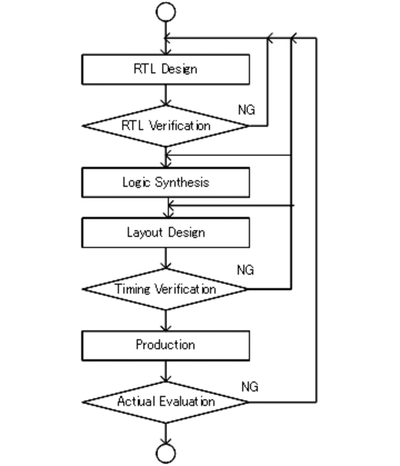
Register transfer level (RTL) design: This process prepares the inner circuit design of the ASIC. The circuit’s implementation method and design intent are described in a circuit diagram, a timing chart, or the like to be included in the design specifications based on which the system’s function and operation are rendered into a model using a hardware description language, such as Verilog HDL or VHDL, at the register transfer level (RTL) for specifying processes between memory devices called flip-flops more abstract than logic circuits4).
Register transfer level (RTL) verification: This process verifies the accuracy of the RTL model designed in the RTL design process. This process uses logic simulation, formal verification, and other technologies to ensure that the design conforms to the specified specifications.
A design not conforming to the specifications will be returned to the RTL design process for modification. This process includes creating a verification environment and implementing a verification plan for a test model and the like.
Logic synthesis: This process converts the RTL model into a physical gate-level netlist. This process converts a high-level abstracted design into an actual logic gate representation. Design data converted into this logic gate representation is called a netlist. Essential considerations for this conversion include circuit optimization, area/performance tradeoffs, and power consumption minimization.
Layout design: The layout design process consists of placing and wiring intra-ASIC physical components (such as transistors and wiring) based on a netlist obtained by logic synthesis. This process takes place at the semiconductor vendor. In this process, a design undergoes physical implementation for integration into a netlist with physical requirements considered, including chip area efficiency, wiring optimization, heat control, and power distribution.
Timing verification: Timing verification is a process that guarantees that the designed circuit meets specific timing requirements. Following verification by the semiconductor vendor, this process takes place on the designer’s side. This process verifies each timing requirement based on clock or signal propagation delay information, which reflects the information about the placing and wiring performed in the layout process. A circuit not meeting a specific timing requirement will be returned to the layout process for a review of the placing and wiring on the circuit. Should the timing requirement remain unmet even after that, the circuit will go back to the RTL design process.
Manufacturing: This is the ASIC manufacturing process. Based on the design data generated through the preceding processes, the ASIC goes into manufacturing at the semiconductor manufacturing factory. The manufactured ASICs undergo the functional test and quality verification processes before shipment.
Device evaluation: This process evaluates the manufactured ASIC mounted on the product. Functional, performance, and environmental endurance evaluations and the like are performed. This process ensures that the ASIC achieves the function, performance, and reliability to the specifications.
2. Challenge during ASIC remake
2.1 Design asset issues
The design assets of ASICs developed in the past are often partially missing or incomplete and have insufficient accuracy. What is meant here by design assets includes the design specifications, circuit diagram, RTL, verification environment, verification results, and various review results documents created through each process described in Subsection 1.4 “Typical ASIC Development Flow.” The insufficiency of these design materials may cause a serious impediment to the implementation of the ASIC remake. Moreover, design asset uncertainties may arise from the insufficient expertise of engineers or teams involved in past designs. In particular, the non-existence of documented design intent or process will make it more challenging to check the original circuit for accuracy and add modifications as necessary during the ASIC remake.
Moreover, intellectual property compliance is also important. An ASIC remake project includes reconfirming the rights associated with the patents and other intellectual properties used in the original design. Especially in the case of an expired or unrenewed license contract, the situation must be handled in cooperation with the Legal Affairs Department.
2.2 Technical issues
2.2.1 Asynchronous circuit issues
Asynchronous circuits had been widely used in many obsolete ASICs. On the one hand, asynchronous circuits have the advantages of lower power consumption and higher performance and circuit efficiency than their synchronous counterparts. On the other hand, they have the following disadvantages:
- Metastability risk: Where an asynchronous signal is received by a flip-flop or some other memory device, the so-called metastable period may occur during which the signal goes into an unstable state4,5), posing a risk that may seriously affect system reliability. Therefore, when an asynchronous signal is received by a flip-flop or some other memory device, an appropriate synchronization circuit must be inserted.
- Increased design complexity: An asynchronous circuit requires a design that considers the real-time timing between signals, including the effects of individual variations or temperature and voltage changes. As a result, the overall design complexity increases, negatively affecting maintainability and scalability.
- Difficulty in verification coverage establishment: An asynchronous circuit must be verified for behavior with consideration given to the timing in real-time, including the effects of individual variations or temperature and voltage changes. However, it is difficult to verify all possible combinations using RTL verification. The common practice is to verify only representative combinations with the timing. As a result, RTL verification can sometimes fail to achieve exhaustiveness. The same is the case with timing verification. A timing verification tool can automatically determine only the following three conditions: cases of the maximum and minimum signal delay times with a case of a typical signal delay time in between. For all other cases, the designer must rely on desktop calculations to make judgments, running the risk of failing to achieve the exhaustiveness of the timing verification.
Therefore, if an obsolete ASIC designed as an asynchronous circuit is remade as such, the risk of defect inclusion runs high because of high design complexity. The design must be examined for validity and compatibility based on device-evaluation waveform measurement or running test results. As a result, any problem during the device evaluation would pose a high risk for the ASIC to go back to the logic synthesis or layout design phase or, in the worst case, to the RTL design phase. Should the risk become a reality, a significantly increased manufacturing cost and period would pose a problem.
2.2.2 Synchronization redesign issues
As the times progressed, semiconductor processes became finer with increases in ASIC circuit sizes. As a result, the disadvantages of asynchronous circuits grew to outweigh their advantages. In 2003, the Semiconductor Technology Academic Research Center Inc. published the RTL Design Style Guide to standardize designer-dependent description styles and design techniques for synthesis, RTL verification, and timing verification for higher readability and currency. After the Style Guide became the de facto industry standard, asynchronous circuit designs, deemed non-recommendable in the Style Guide6), gradually went out of adoption. Today, they have lost their mainstream position to synchronous designs. Unlike asynchronous circuits, synchronous circuits need not be designed and verified in real-time units. Synchronous circuits are advantageous because their behaviors can be exhaustively covered by design and verification on a clock-by-clock basis.
On the other hand, when an obsolete ASIC designed as an asynchronous circuit is redesigned into a synchronous circuit, the problem is that the redesigned synchronous circuit behaves differently from the original asynchronous circuit. Examples of specifics are explained below, referring to Fig. 3, which shows a typical asynchronous circuit adopted as an obsolete ASIC.
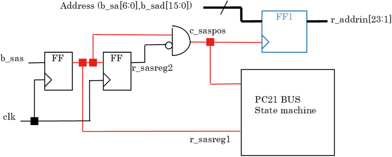
The asynchronous circuit in Fig. 3 has the following two problems:
- The external signal b_sas is latched by a flip-flop (FF). However, with no synchronization-purpose serializer inserted, the risk is that the so-called metastable state may occur, during which the signal becomes unstable4,5). The resulting metastability may propagate via the red line to the PC21bus state machine, posing the risk of destabilizing this state machine’s behavior.
- With a signal other than clock (clk) connected to the clock terminal of the blue flip-flop (FF1), r_addrin[23:1], the output of the blue flip-flop (FF1), is out of sync with the clock, adding complexity to the verification coverage establishment and timing verification of the downstream circuit that uses this signal.
Fig. 4 shows an example of modifying the asynchronous circuit in Fig. 3 into a synchronous circuit to solve the above problems. The synchronous circuit in Fig. 4 solves the problems with the asynchronous circuit in Fig. 3 as follows, respectively:
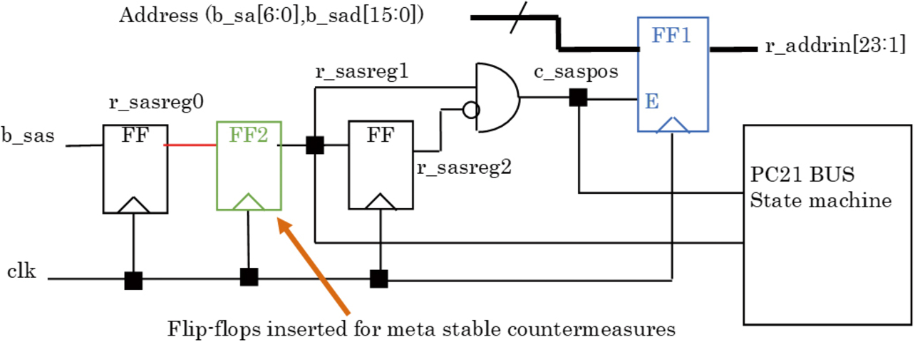
- Build a synchronization-purpose serializer by inserting a green flip-flop (FF2) to bring the external signal b_sas into synchronization. As a result, metastability occurs only within the section indicated in the red line. With no metastability propagation to the PC21bus state machine downstream, the state machine concerned will not show unstable behavior.
- Replace the blue flip-flop (FF1) with one bearing an enable terminal E. Connect the clock signal (clk) to the clock terminal and connect the c_saspos signal, which was connected to the original clock terminal, to the enable terminal E. As a result, r_addrin, the output signal of the blue flip-flop (FF1), comes into sync with the clock, allowing easier verification coverage establishment and timing verification.
In this case, the problem is that the added synchronization-purpose flip-flop causes the r_sasreg1 signal or c_saspos signal output to be delayed by one clock cycle, resulting in an operation different than in the original asynchronous circuit. As explained in Subsection 2.1 “Design Asset Issues,” design assets for obsolete ASICs involve accuracy risks, raising the risk of failure to determine accurately the effects of operation timing change due to synchronization. Moreover, if there is more than one point when the operation timing changes because of synchronization, the effects will interact and become even harder to determine.
2.3 Challenge during ASIC remake
The conventional assumption for ASIC remake has been that the “Synchronization Redesign Issues” in Sub-subsection 2.2.2 cannot be solved as long as the “Design Asset Issues” in Subsection 2.1 remain unsolved. Hence, the standard practice has been to remake an asynchronous circuit into another asynchronous one. As a result, defects identified in the device evaluation mentioned in Sub-subsection 2.2.1 “Asynchronous Circuit Issues” led to iterations, whereby multiple ASIC remake projects experienced problematically significant increases in the development period and cost from the planned levels.
Then, the present author and colleagues propose an ASIC remake method that can solve the “Synchronization Redesign Issues” in Sub-subsection 2.2.2 despite the “Design Asset Issues” in Subsection 2.1 as a solution to the problems with the conventional method. In other words, they propose a solution capable of sufficiently verifying the effects of operation timing change due to synchronization.
3. ASIC remake method proposed herein
The method proposed herein modifies an asynchronous circuit into a synchronous circuit to avoid the challenges in the conventional ASIC remake method as presented in Subsection 2.3 “Challenge during ASIC Remake.” In other words, the method uses the currently mainstream synchronous design approach6) to remake an obsolete ASIC developed in the asynchronous design approach. It aims to reduce the risk of iterations as a challenge in the conventional ASIC remake method. Besides, the method proposed herein adds new tasks to the RTL verification to solve the challenge of failure to determine sufficiently the effects of operation timing change due to synchronization, that is, the factor responsible for avoiding synchronous designs in the conventional ASIC remake method. The following subsections describe the task at each step and the contents to be verified.
3.1 Checking design assets for accuracy
The first task in the RTL design process of the method proposed herein is to check the existing RTL source codes for reliability. As explained in Subsection 2.1 “Design Asset Issues,” existing design assets have the risk of being incomplete with insufficient accuracy. Therefore, an equivalence verification tool is used to check the existing RTL source codes for matching against the post-layout netlist retained in storage at the semiconductor vendor. The equivalence verification tool is intended initially to check the synthesis results or a netlist in the synthesis or layout process for functional equivalence with the original RTL. However, the method proposed herein also uses this tool in the RTL design process to check the RTL for equivalence with the original netlist. Verifying the equivalence between the RTL and the original netlist ensures the accuracy of the existing RTL source codes at a minimum. Fig. 5 shows a typical output of equivalence verification results by Formality7), an equivalence verification tool available from Synopsys Inc.
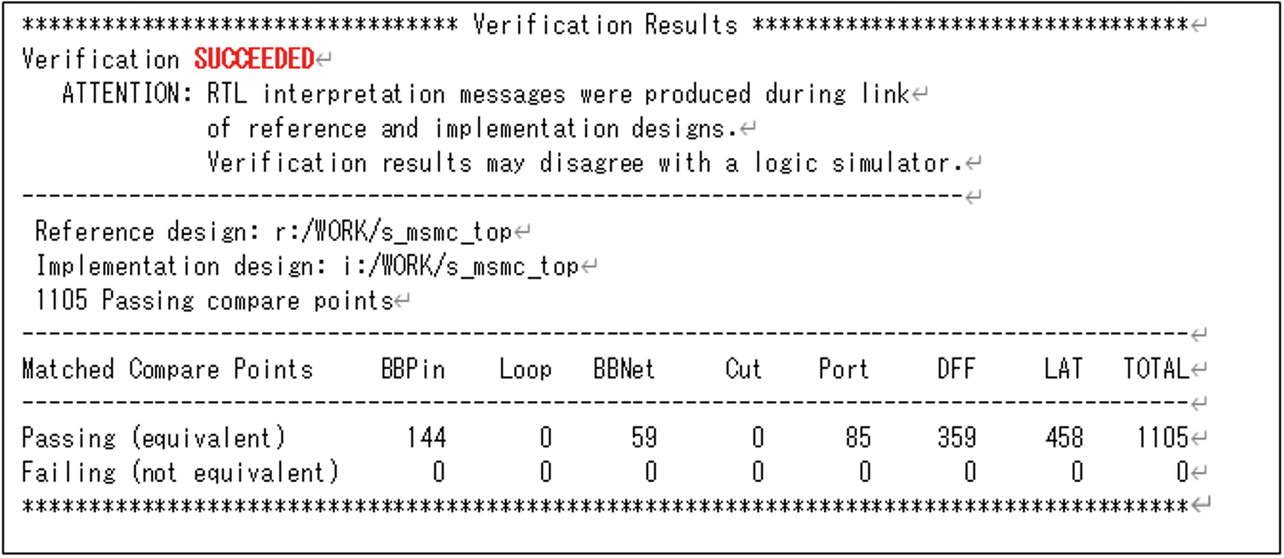
In the case of any inconsistency between the RTL source codes and the netlist retained in storage at the semiconductor vendor, reconsideration must be given, including the continuation of the ASIC remake project. A small number of mismatches can be fixed by modifying the RTL source codes. The RTL source codes cannot be used in the case of numerous mismatches. Alternative measures must be considered, including making a last buy or developing a successor model that will be equivalent or better in function and performance.
3.2 Validating the synchronization redesign
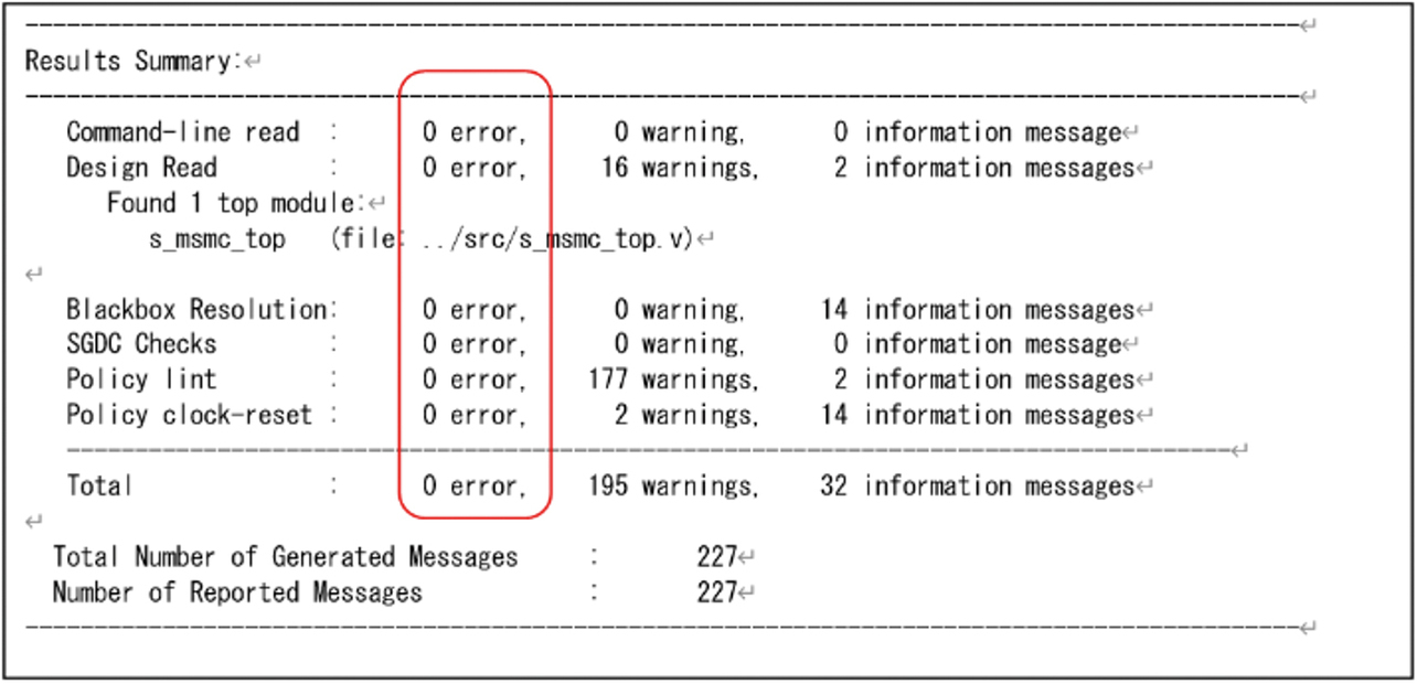
If the RTL source codes and the netlist are verified for correspondence, the next task is to identify asynchronous circuits and implement the synchronization redesign. The recent standard practice in asynchronous circuit identification is to avoid relying on manual work for asynchronous circuit identification and use the so-called clock domain crossing (CDC) checker tool to prevent false negatives due to the reliance on manual work. Similarly, the method proposed herein uses a CDC tool for asynchronous circuit identification. Fig. 6 shows an example of an asynchronous circuit identified using Synopsys Inc.’s SpyGlass CDC8), one of the representative CDC tools.
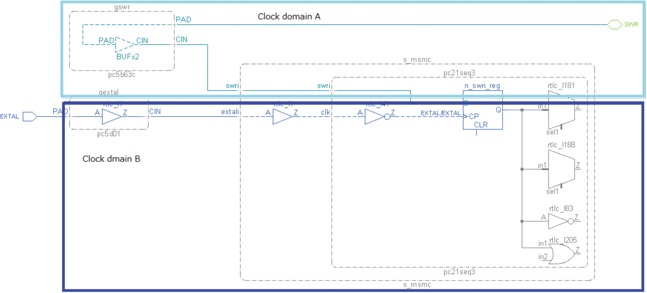
The signals in the light blue and blue boxes (Clock Domains A and B) of Fig. 6 each have a different clock rate than the other, posing the risk that metastability may occur to the output of the downstream-most flip-flop in the blue box. The downstream logic uses the signals as they are, suggesting the possibility that the system may be negatively affected. Any asynchronous circuit identified will be modified into a synchronous circuit, followed by another CDC check to see if the modification is correct. Fig. 7 shows the SpyGlass CDC results output. This task is repeated until all CDC errors are gone, as shown in Fig. 7, or until the errors concerned are confirmed OK. As a result, the validity of the synchronization redesign is guaranteed.
3.3 Checking the synchronization redesign for effects on compatibility
For the RTL verification process, a verification environment shown in Fig. 8 was built to solve the challenge of failure to determine the effects of operation timing change sufficiently due to synchronization, as explained in Sub-subsection 2.2.2 “Synchronization Redesign Issues” in order to ensure functional and performance compatibility.
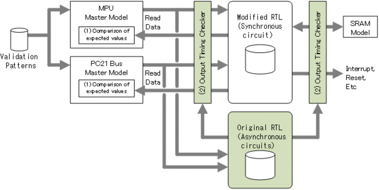
The parts hatched in green are the modules added for the method proposed herein.
The following are the descriptions of the modules in this environment:
- MPU master model: This model generates microcomputer read and write access timings. During read access, this model compares the read data from the modified RTL, the unit under verification, with the expected value shown beforehand in the verification pattern to determine the appropriateness of the read access made.
- PC21bus master model: This model generates single and burst read and write access timings in our proprietary PC21bus protocol. During single and burst read accesses, this model compares the read data from the modified RTL, the unit under verification, with the expected value shown beforehand in the verification pattern to determine the appropriateness of the read access made.
- Modified RTL: A module under verification. A synchronization redesign version of the RTL of the ASIC under remake based on the RTL design mentioned above. Used for data exchanges between the PC21bus master and MPU master models via an external SRAM.
- SRAM model: This model contains data in a specified address for write access from the modified RTL. Conversely, this model returns the data in the specified address for read access from the modified RTL.
- Original RTL: A module added by the method proposed herein. In other words, it is the RTL of the ASIC under remake. This module is functionally the same as the modified RTL. However, it consists of asynchronous circuits and has a different signal output timing accordingly. As shown in Fig. 8, this module is also connected to the input signal from the PC21bus master model as in the case of the modified RTL model. However, the output signal from this model is connected not to the master models but to the output timing checkers explained below. Hence, the read data from this module is not used to compare the expected value with each master model’s value.
- Output timing checkers: Modules added for the method proposed herein. As shown in Fig. 8, these modules are connected to the original and modified RTL module output signals and check the two modules’ differences in signal value and output timing on a clock-by-clock basis. In the case of an output signal difference exceeding a specific clock count or a value gap, these modules issue a simulation error notification.
In the method proposed herein, the MPU master model, PC21bus master model, and others simultaneously access the modified and original RTL modules. Regarding read accesses, each model compares the read data from the modified RTL module with the expected value as in a standard RTL verification. Moreover, the output timing checker modules added by the method proposed herein compare the outputs from the original and modified RTL modules. An OK judgment occurs if the expected value checked by each model and the output timing difference between the output timing checker modules fall within a specific clock count. Suppose that the output timing difference between the output timing checker modules exceeds a specific clock count while the results of the expected value checks by the models are in agreement. Then, a Not OK judgment occurs, prompting a modification to the modified RTL module. Furthermore, suppose that the output timing difference between the output timing checker modules falls within a specific clock count while the results of the expected value checks by the models are in disagreement. In that case, the chance is high that the cause of the problem is the existing verification pattern. The verification pattern is checked and will be modified as necessary. The models also access the external SRAM. For these accesses, similarly to the case of internal accesses, the output timing checker modules compare the outputs from the modified and original RTL modules to the SRAM model to determine the output timing difference on a clock-by-clock basis. For any necessary function other than the above, the output timing checkers compare the output timings to determine if the output timing difference is OK.
The rest of this subsection describes the method of output timing comparison by the output timing checkers, one of the features of the method proposed herein. As mentioned above several times, when an asynchronous circuit is turned into a synchronous design, the circuit output has a timing delay of a few clocks behind the original asynchronous circuit output. The tolerance for the clock count difference depends on the system: there is no problem as long as the MPU, memory, and other access times remain unchanged. In the case of an unacceptable output difference, the internal circuit must be modified to change the output timing. In many cases of remake developments, the ASIC semiconductor processes used for the remake are finer than the original ASIC semiconductor processes. As a result, propagation delays occur earlier in the internal circuit, whereby an output timing change by an internal circuit modification is possible in many cases.
In the case of an unacceptable output difference plus an unchangeable output timing, the customer would be unable to use the remade ASIC in the same way as before the remake. Hence, reconsideration must be given to whether to continue with the remake project.
For output timing comparisons, a method known as assertion-based verification (ABV) is used to perform automatic comparisons in operating clocks. The ABV method assumes that in-circuit or interface signal behaviors should be described using a dedicated assertion language such as System Verilog Assertion (SVA) or Property Specification Language (PSL)9). The method proposed herein uses the original RTL internal and output signals. Therefore, the behaviors of the internal circuits or interface signals need not be newly described using an assertion language like SVA or PSL. Fig. 9 shows the descriptions necessary for the method proposed herein.
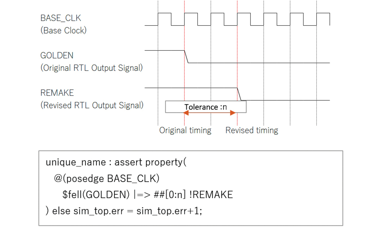
As shown in Fig. 9, the modified RTL and original RTL outputs are compared clock-by-clock only to state the permissible number of clock cycles for a signal difference. As such, this method can be applied relatively easily without the burden of learning assertion description languages.
Thus, the method proposed herein compares the output of the original RTL, an asynchronous circuit, with that of the modified RTL, one remade into a synchronous circuit, on a clock-by-clock basis to ensure functional and performance compatibility within the range of a few clock cycles.
3.4 Verification coverage establishment
This section concludes by describing verification coverage establishment. As also explained in Sub-subsection 2.2.1 “Asynchronous Circuit Issues,” an asynchronous circuit must be verified for timing, including individual variations or temperature and voltage changes. However, these factors could not be considered in the RTL verification. Only representative combinations with timings were verified with little weight placed on the RTL verification’s exhaustiveness. On the other hand, a synchronous circuit can generally be almost exhaustively verified using the verification pattern with timings combined on an appropriate clock-by-clock basis to suit the circuit structure. The effects of individual variations or temperature and voltage changes, which must be considered for an asynchronous circuit, are automatically determined by an analysis tool during timing verification.
When verifying an existing verification pattern using the verification environment shown in Fig. 8, the method proposed herein uses a coverage measurement tool to measure the verification coverage. This method guarantees quality by adding verification patterns and continuing coverage measurement until sufficient verification coverage is reached as in the case of verifying a typical synchronous circuit. Fig. 10 shows typical coverage measurement results obtained by Xcelium10), a logic simulator available from Cadence Inc.
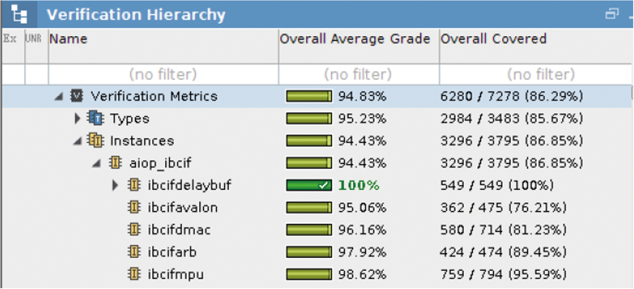
Even if a coverage measurement result is 100%, whether the verification coverage is sufficient must be studied based on use cases and actual RTLs. Nevertheless, when any coverage measurement result is not 100%, it at least indicates that some codes remain unverified. Suppose the original RTL still contains so-called dead codes, unwanted codes that do not work. In that case, the coverage will never reach 100%, no matter how many verification patterns may be added. Each time the coverage fails to reach 100%, the designer must determine whether the cause is verification pattern insufficiency or whether the code at issue is a dead code.
In the method proposed herein, an obsolete ASIC, an asynchronous circuit, is redesigned into a synchronous circuit. The method proposed herein characteristically compares the output of the pre-redesign RTL (an asynchronous circuit) with that of the RTL redesigned into a synchronous circuit on a clock-by-clock basis to ensure functional and performance compatibility within the range of a few clock cycles. This method guarantees quality by adding verification patterns and continuing coverage measurement until sufficient verification coverage is reached as in the case of verifying a typical synchronous circuit. As a result, the method enables ASIC remaking with stable quality, convincing us that it allows us to fulfill the responsibility of supplying customers.
4. Effectiveness and future challenge of the method proposed herein
4.1 Effectiveness
In the past, the present author experienced four ASIC remake projects using the conventional ASIC remake method. Table 1 shows the results.
| No. | Application | Means of implementation |
Device evaluation results |
Market defect |
|---|---|---|---|---|
| 1 | Ladder engine | FPGA | Many modifications | Occurrence×1 6-month shipment suspension |
| 2 | Bus control ASIC | ASIC | Board modification×1 | No problem |
| 3 | Network control ASIC | ASIC | ASIC rework×2 Board modification×1 | No problem |
| 4 | Counter control ASIC | ASIC | No problem | No problem |
For the ladder engine ASIC remake project shown in the first row of Table 1, the present author gave up a remake into an ASIC at the prospect of many iterations and switched to a remake into a field-programmable gate array (FPGA). As a result, a market defect occurred, leading to about half a year-long shipment suspension. In the subsequent remake projects, no market defect occurred. However, in the bus control ASIC project shown in the second row of Table 1, a defect was detected in the pre-market launch device evaluation and had to be addressed through ASIC reworks and board modification. The counter control ASIC remake project in the fourth row of Table 1 did not involve the output comparison with the original RTL module, which was explained in Section 3 “ASIC Remake Method Proposed Herein.” With the internal circuit modified into a synchronous circuit, this ASIC remake project was a transitional phase from the conventional method to the method proposed herein.
Using the method proposed herein, the present author and colleagues have already implemented six remakes into ASICs and launched products mounted with the remade ASICs into the market. Table 2 shows the results.
| No. | Application | Means of implementation |
Device evaluation results |
Market defect |
|---|---|---|---|---|
| 1 | Bus control ASIC | ASIC | No problem | None |
| 2 | Bus control ASIC | ASIC | No problem | None |
| 3 | Network control ASIC | ASIC | No problem | None |
| 4 | Bus control ASIC | ASIC | No problem | None |
| 5 | Bus control ASIC | ASIC | No problem | None |
| 6 | Bus control ASIC | ASIC | ASIC rework×1 | None |
As shown in Table 2, no post-launch defect was reported, including the abovementioned defect. Thus, the method proposed herein achieved stable quality and can be regarded as a highly effective development method.
On the other hand, in the bus control ASIC project in the sixth row of Table 2, a defect was detected in the prelaunch device evaluation, forcing the ASIC to be reworked. The cause was that the responsible staffer was aware of a difference between the original and modified RTLs in the verification environment shown in Fig. 7 but misjudged the difference as acceptable. Before the market launch, this defect was fixed to remove the difference between the original and modified RTLs. This case suggests that any difference between the original and modified RTLs should be checked and judged by more than one person.
4.2 Future Challenge
The present author and his team are currently implementing two more ASIC remake projects using the method proposed herein. During the process, it was confirmed that the number of man-hours required to achieve exhaustiveness has significantly increased along with the increasing circuit scale. The main cause of this increase is the existence of codes that never get executed, that is, so-called dead codes explained at the end of Subsection 3.2 “Verification Coverage Establishment.” The term “dead code” refers to a code block never executed because of a certain permanently false condition and never reached by the program flow. In ASIC developments, dead codes are automatically removed through logic synthesis and usually deemed noninfluential on the circuit’s size, behavior, and performance. Hence, no special measures have been implemented. As a result, numerous man-hours are required to determine whether coverage failures in verifications are due to verification pattern insufficiency or dead code. Given the expanding trend in the circuit scale for ASIC remake, the future challenge would be to study an effective method of dead code detection to allow continued application of the method proposed herein.
5. Conclusions
This paper discussed the need for ASIC remake as a method to prepare for ASIC discontinuation. The paper explicitly presented a challenge during ASIC remake based on design asset issues and technical issues and proposed a new method to address these challenges. For the method proposed herein, the present author presented a specific procedure for remaking an asynchronous circuit widely adopted for obsolete ASICs into a synchronous circuit, the current mainstream for ASICs. The present author showed it possible to transition to a synchronous circuit and simultaneously ensure functional and performance compatibility while taking flexible and effective measures for the abovementioned challenges. Regarding specific achievements, the present author and colleague used the method proposed herein to remake six ASICs and confirmed the method’s effectiveness in providing stable and high-quality products. From these observations, the present author concludes that the semiconductor industry can fulfill the responsibility of supplying customers by supplying stable and high-quality ASICs through flexible and continual adaptation to rapidly changing situations.
However, the existence of dead codes emerged as the cause of the increasing verification man-hours along with the increasing circuit scale. How to detect dead codes efficiently remains a future challenge. The present author expects that it will be necessary in the future to establish more efficient development methods through continuous application of the method proposed herein in addition to improving dead code detection methods.
References
- 1)
- Nikkei. “Fujitsu to Sell Mie Semiconductor Factory to Taiwan UMC for \57.6 Billion.” (in Japanese), Nikkei Inc. https://www.nikkei.com/article/DGXMZO32425480Z20C18A6TJC000/ (Accessed: Feb. 7, 2024).
- 2)
- Renesas Electronics Corporation. “Notice of Closure of Yamaguchi Factory.” (in Japanese), News. https://www.renesas.com/jp/ja/about/press-room/notice-regarding-closure-yamaguchi-factory (Accessed: Feb. 7, 2024).
- 3)
- Commerce and Information Policy Bureau. “Semiconductor and Digital Industrial Strategies.” (in Japanese), Ministry of Economy, Trade and Industry. https://www.meti.go.jp/press/2023/06/20230606003/20230606003-1.pdf (Accessed: Feb. 7, 2024).
- 4)
- Toshiba Device & Storage Co., Ltd. “Protection against Metastability.” (in Japanese), Precautions for Use of CMOS Logic IC. https://toshiba.semicon-storage.com/jp/semiconductor/knowledge/e-learning/cmos-logic-usage-considerations/usage-11.html (Accessed: Jan. 22, 2024).
- 5)
- Intel Corporation, AN 42: Metastability in Altera Devices, Ver. 4.0 (2019). Accessed: Jan. 22, 2024 [Online], Available: https://www.intel.com/content/www/us/en/content-details/653636/an-42-metastability-in-altera-devices.html?wapkw=an42
- 6)
- IP Technology Development Office, Design Technology Dept., STARC. RTL Design Style Guide for Verilog HDL, 1st Ed., Semiconductor Technology Academic Research Center Inc., 2003, Ch. 1, pp. 17-18.
- 7)
- Synopsys, Inc. “Formality Equivalence Checking.” (in Japanese), Synopsys. https://www.synopsys.com/ja-jp/implementation-and-signoff/signoff/formality-equivalence-checking.html (Accessed: Feb. 21, 2024).
- 8)
- Synopsys, Inc. “SpyGlass CDC.” (in Japanese), Synopsys. https://www.synopsys.com/ja-jp/verification/static-and-formal-verification/spyglass/spyglass-cdc.html (Accessed: Feb. 21, 2024).
- 9)
- J. Bergeron et al., Verification Methodology Manual, 1st Ed. (Japanese ver.), CQ Publishing Co., Ltd., 2006, pp. 53-112.
- 10)
- Cadence Design Systems. Inc. “Xcelium Logic Simulator.” (in Japanese), Cadence. https://www.cadence.com/ja_JP/home/tools/system-design-and-verification/simulation-and-testbench-verification/xcelium-simulator.html (Accessed: Feb. 21, 2024).
The names of products in the text may be the trademarks of each company.
Synopsys, Formality, and SpyGlass are the registered trademarks or trademarks of Synopsys, Inc., in the United States and other countries.
Cadence and Xcelium are the registered trademarks or trademarks of Cadence Design Systems, Inc., in the United States and other countries.
Altera is the trademark of Intel Corporation or its subsidiaries.