


Development of High-Capacity Power Supply for FA, Contributing to a Decarbonized Society
- Power supply
- High-capacity
- Avoiding wiring burnout
- High efficiency
- Carbon neutral
Amidst efforts for a carbon-neutral and decarbonized society, manufacturing automation speeds up because of the declining labor force and satellite factory promotion. The growing use of electric, safety, and IoT devices in manufacturing raises concerns about increased energy consumption and growing occupancy of space within equipment and control panels. To address these issues, power supplies are expected to evolve, becoming smaller yet higher capacity and more efficient, enhancing energy productivity of the systems and reducing susceptibility to malfunctions. This time, by applying an LLC converter of the primary series-secondary parallel type to a high-capacity power supply, 95.4% efficiency has been achieved for a 2 kW power supply (S8VK-WA20224), which is a significant improvement over the 88.7% efficiency of a conventional 1.5 kW power supply. Furthermore, the optimal heat dissipation structure has been achieved by a simulation that combines magnetism and heat, resulting in natural air cooling to reduce the failure rate. Focusing also on downsizing devices and control panels equipped with power supplies, the technology to limit the wiring current on the power supply side has been incorporated to reduce the wire diameter used for wiring and the size of the control panel by 10%. This technology can also be applied to high-capacity power supplies exceeding 2 kW and is expected to contribute to further realization of a decarbonized society.
1. Introduction
Efforts are underway toward a decarbonized society to reach carbon neutrality by 2050. Moreover, the manufacturing industry has been acceleratingly automated in recent years against the background of a shrinking working population or the promotion of satellite factories. Along with automation, electrically powered, safety, and IoT equipment or the like has increased, giving rise to the need for their power supply units to have greater capacity.
At the same time, it is required from the perspective of cost and environmental load reduction to avoid scaling up equipment and control panels as much as possible in response to such circumstances. More compact, higher-capacity/higher-efficiency (lower-loss) power supply units become necessary to meet such needs. Miniaturization is also expected to effectively reduce raw material usage for products and greenhouse gas (GHG) emissions from product transportation.
High-capacity power supply units based on existing technologies generate large amounts of heat internally and require forced air cooling. However, forced air cooling has a higher failure rate than natural air cooling when viewed from such a perspective when the fan’s service life expiry or the ingress of dust and other foreign matter is considered. Forced air cooling causes machines to stop more frequently, reducing productivity and increasing devices’ standby power consumption and reducing energy productivity. In other words, it has the problem of increasing GHG emissions.
This paper presents and describes a technology for developing a high-capacity power supply unit that can address the above problems and contribute to control panel miniaturization and GHG emissions reduction.
2. Technical challenges
2.1 Current homogenization for multiple elements connected in parallel
It is currently a widespread practice to adopt half-bridge LLC converters (hereinafter “LLC converters”) for small-to-medium capacity power supply units ranging from approximately 100 W to 1 kW. The reason is that LLC converters can add high efficiency to power supply units through the zero-voltage switching of the primary-side MOSFET and the zero-current switching of the secondary-side diode. However, adopting LLC converters for high-capacity power supply units exceeding 1 kW will lead to causing the high current stress inherent in resonant circuits on power devices or transformers. The following describes the details.
Fig. 1 compares an LLC converter with a full-bridge converter adopted for our existing high-capacity power supply unit in terms of the plot of the waveform of the current flow to their respective secondary-side transformer. The LLC converter had a near-sinusoidal current flow to the secondary side. As such, the LLC converter showed higher peak and effective currents than the full-bridge converter, indicating the former’s likelihood to cause higher current stress than the latter.
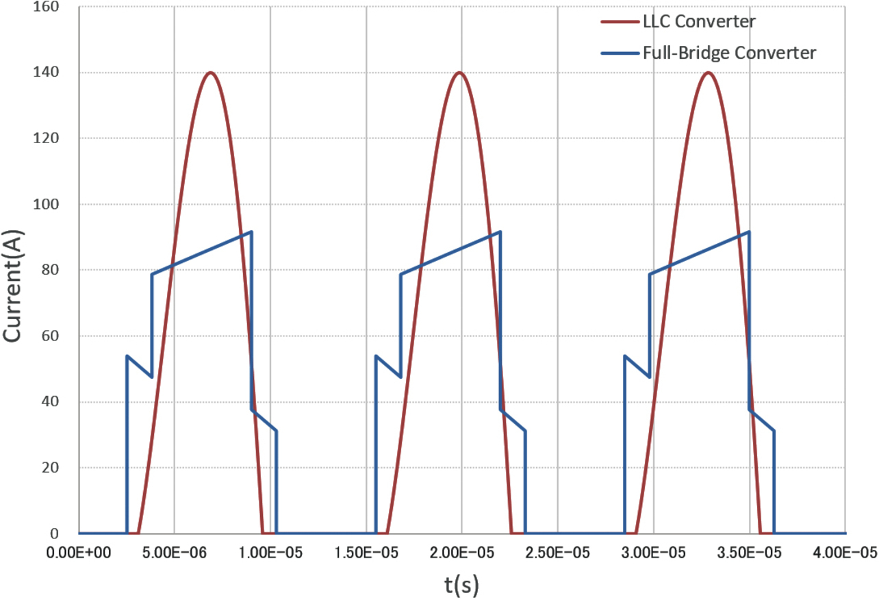
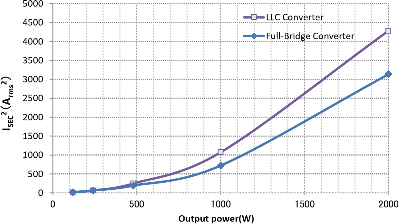
Fig. 2 compares the LLC converter and the full-bridge converter in terms of the square of the effective current to the transformer’s secondary-side winding as measured over the range of power capacity. Semiconductors or transformer windings have a resistance loss proportional to the square of the effective current. It then follows that, with a constant resistance component, a greater loss would result at higher capacities than conventionally.
An example of a solution to avoid high current stress is to connect devices in parallel as in Fig. 3.
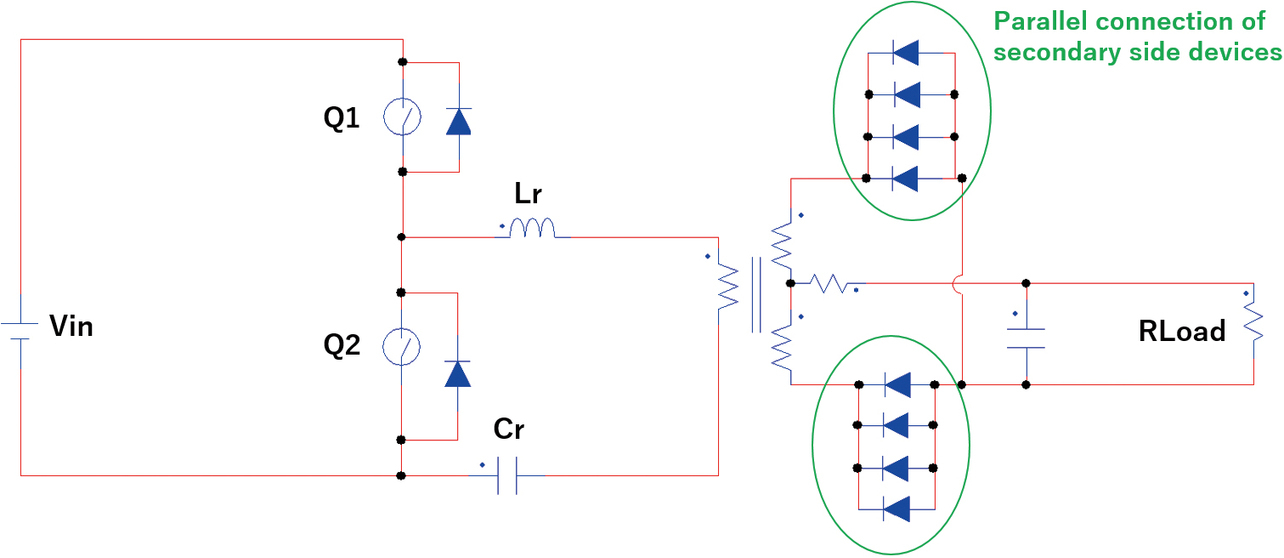
However, this method does not guarantee the current balance in individual devices. The bias of a current to one device leads to reduced efficiency and/or reliability. The challenge in solving this problem lies in splitting and distributing a large current over multiple elements and homogenizing the current flow to each element.
2.2 Compatibility between natural air cooling and miniaturization
Generally, high-capacity power supply units exceeding 1 kW adopt forced air cooling. However, a forced air-cooled power supply unit may cause the problem of reduced energy productivity if shut down because of the fan’s service life expiry or the ingress of dust and other foreign matter. Therefore, needs are mounting for natural air-cooled power supply units.
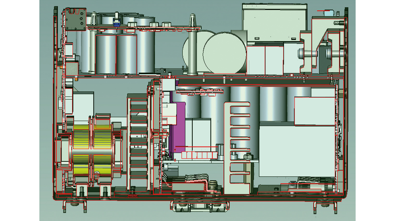
To have both a compact body and natural air cooling, a high-capacity power supply unit needs an optimal heat dissipation structure to cool heat-producing parts. We used to rely on trial and error using prototypes to determine such structures. However, as shown in Fig. 4 (3D data representation of a sectional view of a 2 kW power supply unit), a high-capacity power supply unit consists of many parts and has a complicated structure. Such a power supply unit takes a vast amount of time for development and verification, including the time to create multiple types of prototypes. Hence, we used thermal simulation to consider heat dissipation structures efficiently.
A thermal simulation can produce highly accurate results from correct data on losses in heat-producing components. However, particularly large highly heat-producing magnetic components, such as transformers, make loss calculations challenging, posing the problem of failure to achieve sufficient accuracy for thermal simulation.
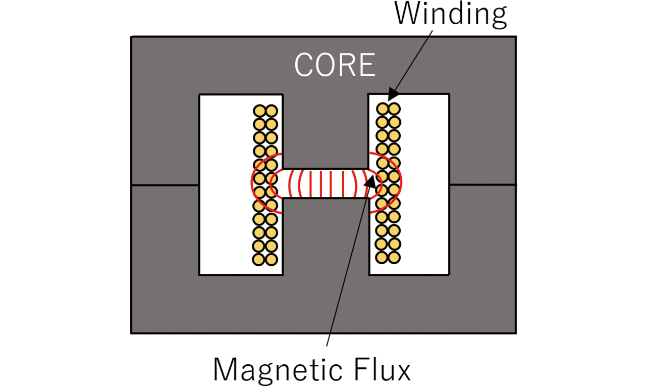
When estimating the loss in a large magnetic component by calculating the loss due to the current flow to the winding (copper loss), we perform the calculation using PC=R×I2, where the R, in other words, the winding resistance value, varies because of such factors as proximity and skin effects. Besides, as in Fig. 5, the leakage flux from the core center gap passes through the winding. As a result, an eddy current flows through the winding, causing eddy current loss. These factors cause the actual loss in the large magnetic component to disagree with the calculation. While it may be an idea to check the loss in an actual device, the abovementioned phenomenon occurs inside the component, making it impossible to observe the current waveform and other parameters. Thus, measuring the actual transformer loss is challenging.
In an attempt to study many trial-and-error patterns in a short time using thermal simulation to identify an optimal heat dissipation structure and achieve the compatibility between miniaturization and natural air cooling, the challenge will be to estimate the loss in the large magnetic component accurately using magnetic simulation.
2.3 Alleviating the constraint of the wire size to use
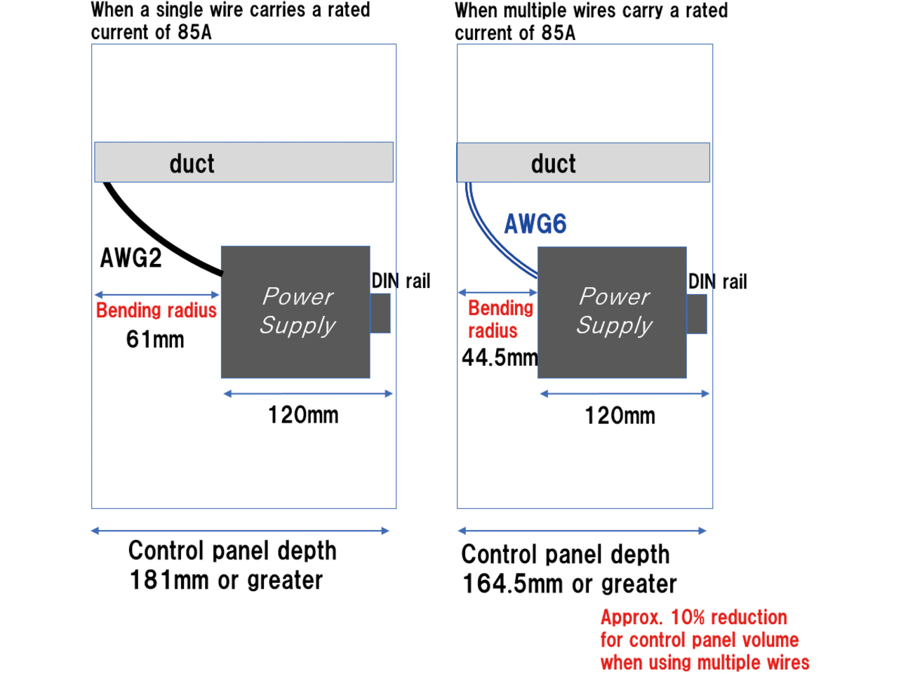
Two (2) kilowatt-class power supply units produce a large current as the output, making it necessary to use thick wires for their wiring. Thick wires have a large bending radius and affect the control panel’s size. When bending the wiring for the purpose of insertion into a duct on the control panel, one can use the following equation to estimate an approximate bending radius:
As shown in Fig. 6, an AWG 2-equivalent wire is necessary to pass, for example, a current of 85 A (that flows at an output capacity of 2 kW and voltage of 24 V). Then, the control panel needs to be 181 mm deep. One of the possible methods of reducing the bending radius is to adopt a multiple-wire configuration using thin wires. Assume using two wires to flow a current of 85 A. Then, the wire size to use will be AWG 6, reducing the depth of the control panel to 164.5 mm or reducing the control panel’s volume by 10% compared with when a single AWG 2 wire is used.
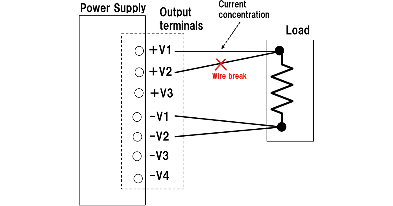
However, the wire size to use must be selected considering the current flow concentration and short-circuit current risks due to such wire breakage as in Fig. 7 from the perspective of safety design against faults. Therefore, the problem remains that there is no choice but to adopt a thick wire.
The challenge in addressing these issues lies in developing a current limiting technology that prevents wiring burnout or any other accident, even in the event of a fault.
3. Solution technology
3.1 Current balancing technology
3.1.1 Circuit systems for split current distribution through a high-efficiency circuit
To solve the challenge presented in Subsection 2.1 and to develop a compact but high-efficiency power supply unit, we need a technology that homogenizes the current flow to each element while splitting and distributing the current over multiple transformers or power devices. Table 1 compares typical split current distribution measures to reduce the current flow to the transformer or semiconductor elements while maintaining the low loss achieved by the zero-voltage switching of the primary-side MOSFET:
| Circuit system | Pros | Cons |
|---|---|---|
| • Full-bridge LLC converter | • Its transformer primary-side current is one-half that of an LLC converter. | • It needs a transformer primary-side number of turns twice that of an LLC converter. • Its current flow to the transformers’ secondary side is similar to that in an LLC converter. Hence, it is left with the problem of current stress on the secondary-side elements (transformer’s secondary-side winding and semiconductors) during high-capacity use. |
| • Parallel-configuration LLC converter • Three-phase interleaved LLC converter |
• It can split and distribute a current over multiple elements. Hence, it can reduce the high current stress on the transformers and devices, enhancing efficiency. • An interleaved system can reduce the secondary-side ripple current and needs less output electrolytic capacitors. |
• Variations in phase transformers or resonant capacitors lead to the loss of the current balance. A complicated circuit must be added for a better current balance. |
| • Primary series-secondary parallel LLC converter | • It can split and distribute a current over multiple elements. Hence, it can reduce the high current stress on the transformers and devices, enhancing efficiency. • The transformers can maintain a favorable current balance even if component variations exist. |
• It cannot reduce the ripple current in the output smoothing capacitor as much as an interleaved LLC converter and hence needs a similar number of output electrolytic capacitors to that in an LLC converter. |
For us to design a power supply unit with a high capacity of 2 kW, the issue of secondary-side current stress remains with the full-bridge LLC converter. Meanwhile, the parallel-configuration LLC converter or the interleaved LLC converter can reduce the current stress but needs an additional active current-sharing circuit or the like to address the issue of current balancing posed by variations in each phase resonant capacitor1). Therefore, these two systems are unsuitable for achieving the required efficiency and reliability for our intended high-capacity power supply unit.
Another alternative is an LLC converter containing multiple transformers with their primary sides connected in series and secondary sides connected in parallel2). Transformers configured to have their primary or secondary windings connected in series or parallel are known as Matrix Transformer. However, this paper refers to this configuration as the primary series-secondary parallel LLC converter. The primary series-secondary parallel LLC converter has its primary-side transformer windings connected in series and hence features a favorable balance between the current flows to the transformers’ respective secondary-side windings3). This system can homogenize the current flow to each element even when component variations exist in a circuit that splits and distributes a large current over multiple elements. Considering this significant advantage, we adopted this system to develop our intended high-capacity power supply unit.
The two important points to remember when at the drawing board are given below. These points concerning the primary series-secondary parallel LLC converter are not mentioned in the references we consulted and are elucidated below in this paper. The first point is to calculate the frequency-gain characteristic and the resonant frequency.
The frequency-gain characteristic significantly relates to the efficiency or output-voltage variable range. Fig. 8 shows an example of the frequency-gain characteristic of an LLC converter. However, the LLC converter changes the switching frequency to control the output voltage. Hence, the Y-axis is not converted to the gain but the output voltage Vo (Vo=1/2×input voltage×gain).
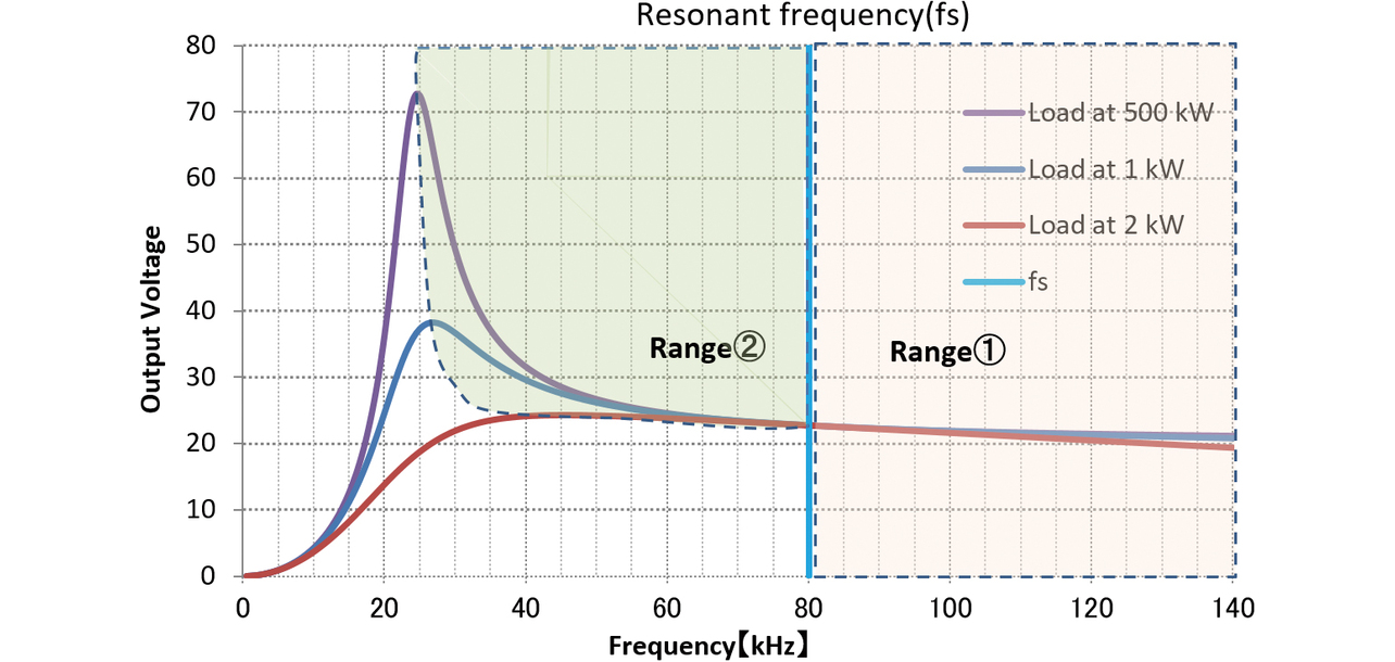
Note that each vertical line in the graph grid represents the resonant frequency (fs). Depending on whether to operate at a frequency above or below it, the LLC converter changes its operation mode. When it operates in Range (1), its primary-side MOSFET switching loss increases, affecting the power supply unit’s efficiency4). Moreover, when the LLC converter significantly fluctuates its switching frequency, its output voltage changes only slightly; in this case, a power supply unit with a variable output voltage may fail to meet its product specifications. When the LLC converter operates in Range (2), its primary-side current increases at lower frequencies, resulting in increased conduction loss4).
To consider these requirements, we calculated the frequency-gain characteristic and resonant frequency in the primary series-secondary parallel LLC converter.
The second point is to check the impact of each component’s variations on the current balance.
The primary series-secondary parallel LLC converter uses multiple transformers for split current distribution to each element. When these transformers’ parameters exhibit variations, we must check how much they affect the current balance. Then, the allowable ranges for the transformer parameters for the balance between the current flows to the individual elements to fall within a target variation range of approximately 5% must be determined to optimally custom design the transformers. Note that this 5% is our design criterion for designing the current balance in a power supply unit circuit.
3.1.2 Frequency-gain characteristic of the primary series-secondary parallel LLC converter
At the outset of considering the primary series-secondary parallel LLC converter, we derived the gain M and the resonant frequency fs, the relations for the frequency-gain characteristic using fundamental harmonic approximation (FHA).
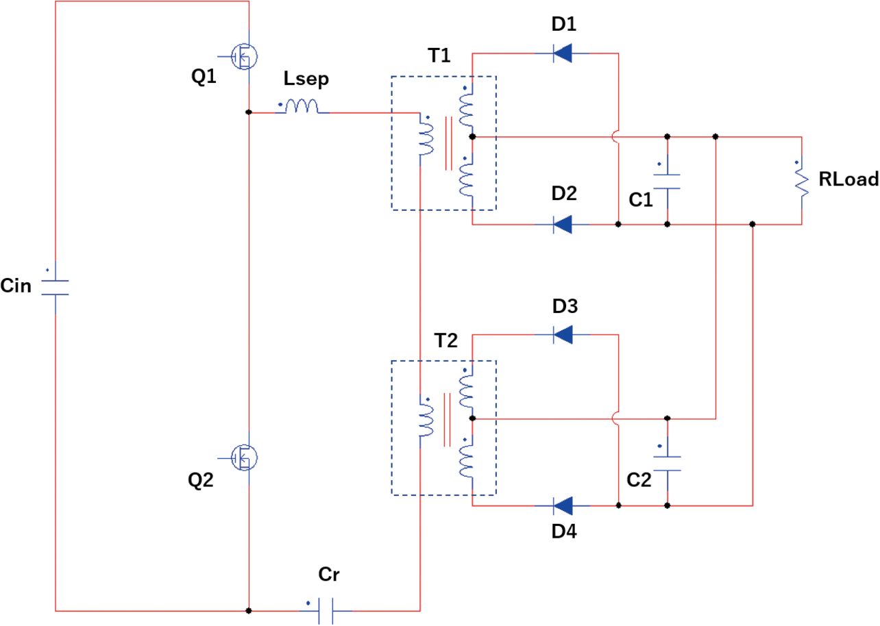
Fig. 9 shows the circuit diagram of this system, wherein T1 and T2 are transformers:
Then, Fig. 10 shows an equivalent circuit converted from Fig. 9 to calculate the gain using FHA:
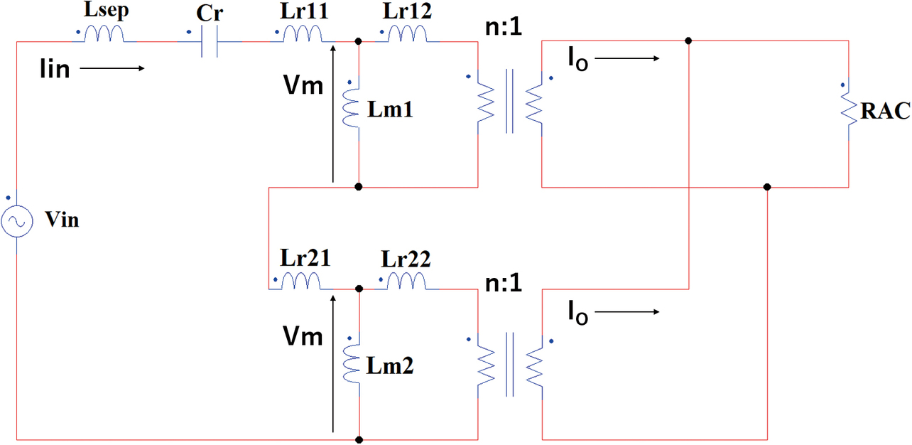
Note here that the symbols in the diagram represent the following, respectively:
Lr11, Lr21: Primary-side leakage inductance of Transformers T1 and T2
Lr12, Lr22: Secondary-side leakage inductance of Transformers T1 and T2
Lm1, Lm2: Magnetizing inductance of Transformers T1 and T2
Cr: Resonant capacitor
Lsep: Inductance for resonance
RAC represents the AC output resistance converted from the output load resistance RLOAD using the following equation:

Calculate the gain M in this equivalent circuit. Let the parameters be as follows for simplification:


Let RAC-generated voltage be Vo to calculate M = Vo/Vin. The following circuit equations are obtained from the equivalent circuit:


From the above equations, the gain M is calculated as follows:

However,


Hence, the resonant frequency fs is given as follows:

Let the DC voltage applied to Cin in Fig. 9 be VinDC. Then, the output voltage Vo is given below using the derived gain M:

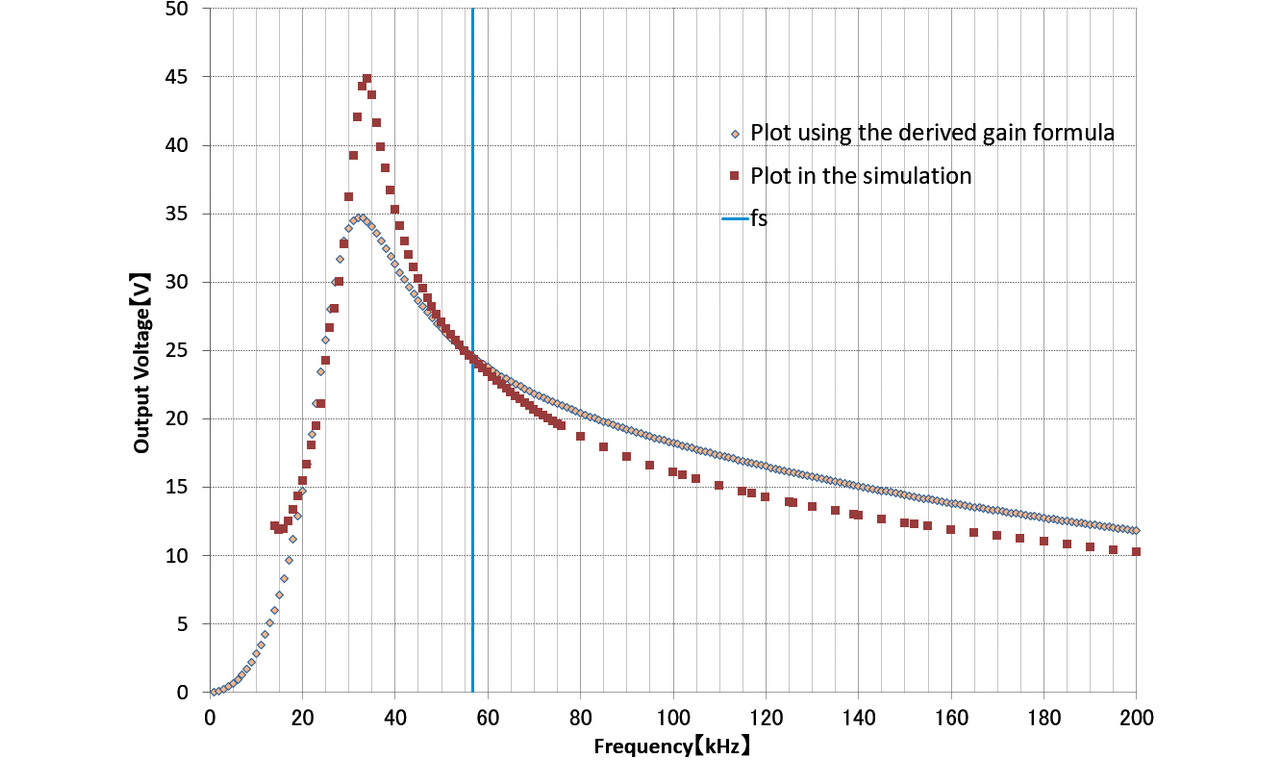
Fig. 11 validates the analysis results by comparison with the simulation results. We used SCALE (Smart Energy Laboratory Co., Ltd.) for the circuit simulation. Fig. 11 shows that the analysis and simulation results are in general agreement, indicating that the achieved accuracy was sufficient to design the primary series-secondary parallel LLC converter.
We used the following parameters for verification:
VinDC=390 V, Lsep=1 uH, Lm=39.7 uH, Cr=376 nF, and RLOAD=282 mΩ
3.1.3 Current balance verification
For the primary series-secondary parallel LLC converter, it is important whether to install external resonant inductors or use each transformer’s built-in leakage inductance. Considering the size of the product, we decided to use each transformer’s built-in leakage inductance as a resonant inductor. Then, the allowance of the inductance and that of the transformer’s built-in leakage inductance would matter to secure the current balance. Therefore, we determined their allowances.
We verified the actual impacts of the variations of the transformer parameters Lp (primary-side inductance) and LLK (transformer’s built-in leakage inductance) on the current balance. Note here that Lp and LLK are related to Lr and Lm as follows:


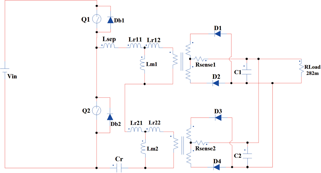
We verified the effective current by assuming Lp=33 uH (Typ) and LLK=7.2 uH (Typ) and giving them variations in the circuit simulation in Fig. 12. We obtained the effective current waveforms of Rsense1 and Rsense2 shown in Fig. 12 to compare their effective currents in Table 2.
| Transformer | Parameter | Case A Parameters unchanged |
Case B1 Lp±10% LLK±10% |
Case B2 Lp±20% LLK±20% |
Case C1 Lp ∓ 10% LLK±10% |
Case C2 Lp ∓ 20% LLK±20% |
|---|---|---|---|---|---|---|
| Transformer (1) | Lp | TYP | +10% | +20% | −10% | −20% |
| LLK | TYP | +10% | +20% | +10% | +20% | |
| I (Rsense1) | 47.6 Arms | 48.29 Arms | 49.92 Arms | 44.74 Arms | 42.09 Arms | |
| Rate of increase in effective current relative to when in balance (Case A) | / | 1.45% | 4.87% | −6.01% | −11.58% | |
| Transformer (2) | Lp | TYP | −10% | −20% | +10% | +20% |
| LLK | TYP | −10% | −20% | −10% | −20% | |
| I (Rsense2) | 47.6 Arms | 46.31 Arms | 44.94 Arms | 50.19 Arms | 54.8 Arms | |
| Rate of increase in effective current relative to when in balance (Case A) | / | −2.71% | −5.59% | 5.44% | 15.13% |
Table 2 shows Case A for the effective currents of Rsense1 and Rsense2 without variations and Cases B1, B2, C1, and C2 for their effective currents with variations: ±10% and ±20% variations to each were the conditions for throwing the currents off balance the most in Case C1 and Case C2, respectively.
The verification results revealed that the transformers’ Lp and Lr with ±20% deviation led to an actual increase in the current flow to the transformer by +15%, which is unacceptable, but that, with deviation of Lp and Lr controlled at or below ±10%, the actual increase in the current flow to the transformer remained within around +5.5%, an acceptable level. The above observations identified the Lp and LLK allowance requirements to satisfy the current balance requirements.
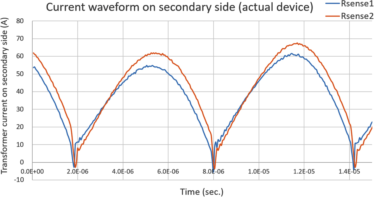
Fig. 13 shows the plots of the current waveforms obtained by preparing the transformers with variations in Table 3 and installing them in an actual device to empirically confirm the simulation’s probability. Fig. 14 shows the plots simulated for the same conditions as that experiment.
| Transformer | Parameter | Variations |
|---|---|---|
| Transformer (1) | Lp | −8% |
| LLK | +5% | |
| Transformer (2) | Lp | +7% |
| LLK | −7% |
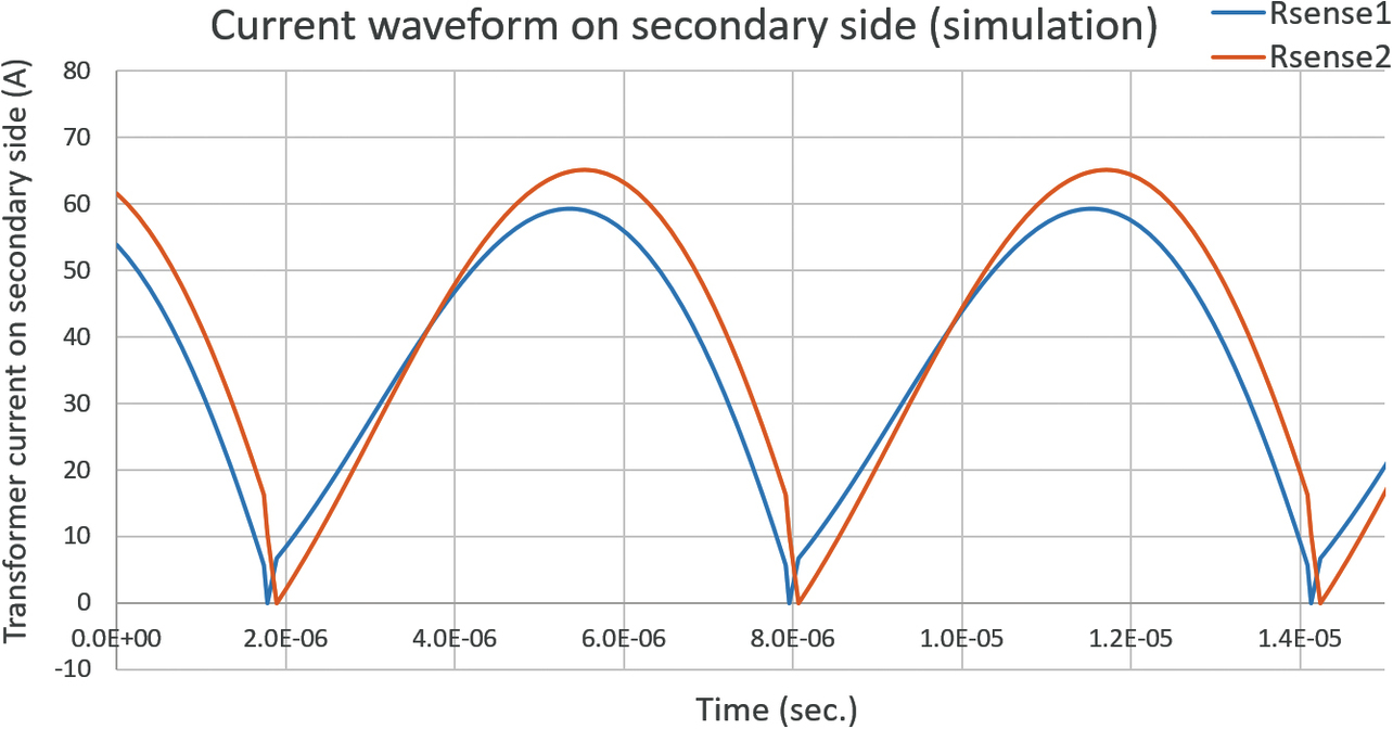
It turned out that the simulation and the actual device agreed well for, say, the differences between the current flows to the two transformers, albeit some differences between absolute values. We can say that the simulation presented above is suitable to consider the circuit.
3.1.4 Verification of the loss improvement effect achieved by the primary series-secondary parallel LLC converter
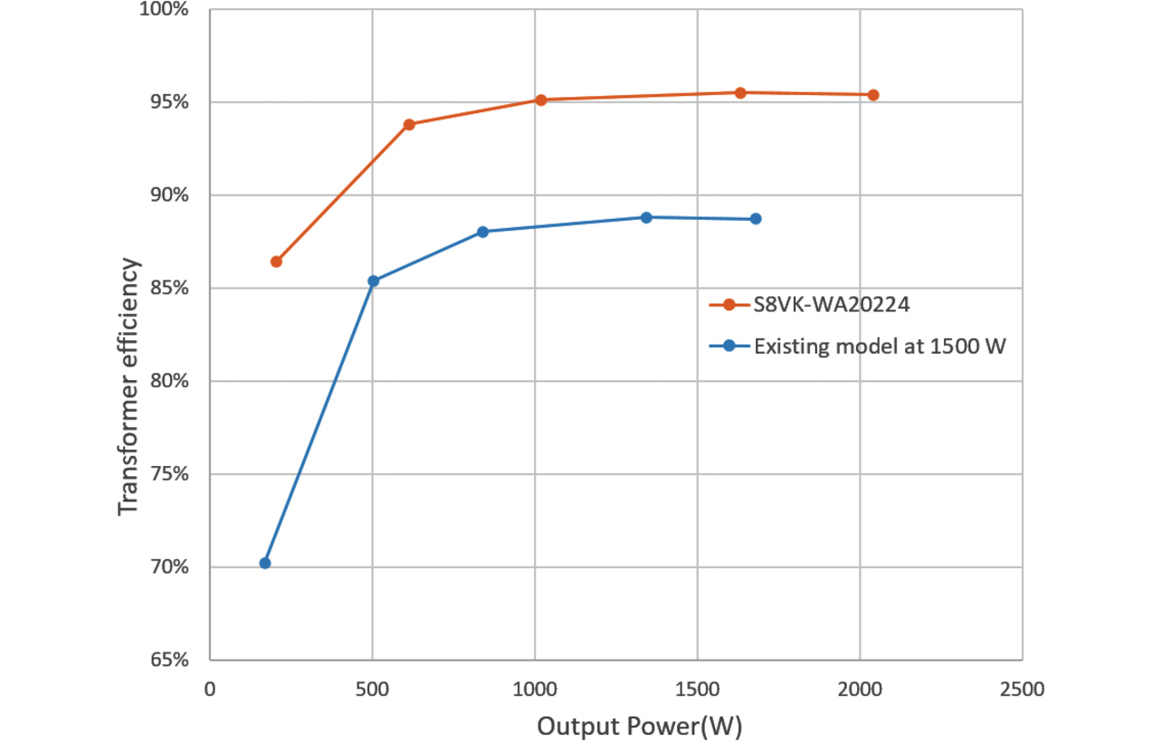
We adopted a high-efficiency circuit system for split current distribution over multiple paths to reduce the current stress on the transformers and semiconductors. As a result, the efficiency of the DC-DC converter unit improved, achieving a product efficiency of 95.4%, as shown in Fig. 15. This value is a significant improvement relative to the 88.7 percent efficiency of our existing high-capacity model (1500 W).
3.2 Loss calculation using magnetic simulation
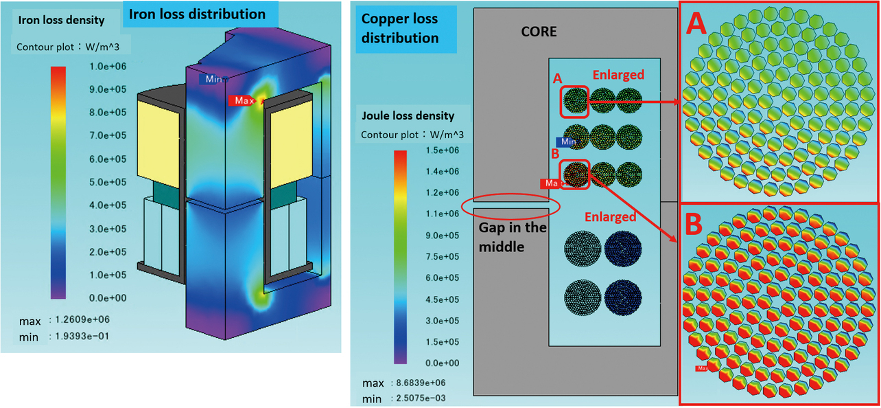
We calculated the losses in the individual elements to consider the heat dissipation structure based on thermal simulation. Given that losses in transformers and other large magnetic components are hard to estimate accurately by desktop calculation, as explained above, we calculated these losses using magnetic simulation. Fig. 16 shows the simulation results. We used JMAG (JSOL Corporation) for the magnetic simulation.
We paid attention to the following points to improve the accuracy of the loss estimation based on the magnetic simulation:
(1) As shown in Fig. 16, the winding near the core center gap (the winding in Pane B of the Figure) exhibited a significant loss, while the winding distant from there (the winding in Pane A of the Figure) showed a minor loss. Thus, the eddy current loss caused by the leakage flux from the center gap was observed to affect the simulation. To improve the eddy current loss estimation accuracy, we created the simulation models to reproduce the relative positions of the core center gap and the windings as close to those in the real transformer as possible.
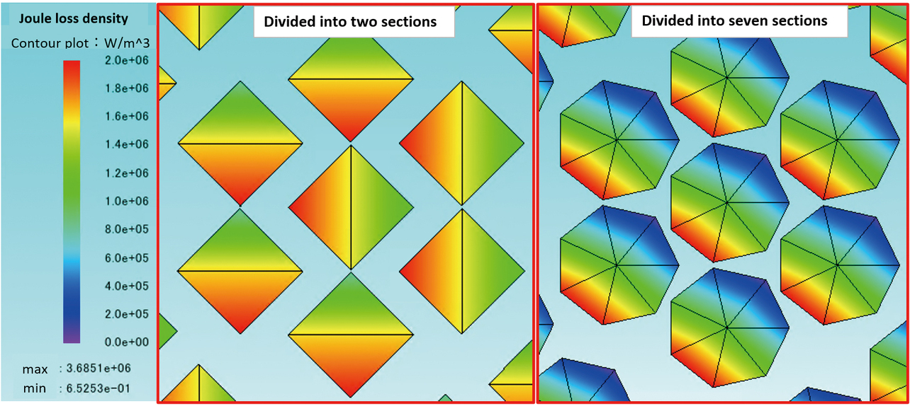
(2) The mesh size near the winding conductors or core gap matters when reproducing the influence of the proximity and skin effects. More specifically, when the mesh size near the conductors was defined by two equal halves in a divided whole, as shown in Fig. 17, the conductor loss distribution did not sufficiently reflect the influence of the proximity effect. On the contrary, when the mesh size was defined by seven equal parts in a divided whole, the influence of the proximity effect was observed in the simulation, indicating an improvement in loss calculation accuracy. As regards the skin effect, its influence did not appear in the simulation with the wire size to use being as sufficiently small as 0.1 mm. However, too small a mesh size would increase the required simulation time. Therefore, we ensured the simulation speed and accuracy compatibility by checking with the loss distribution for the minimum mesh size to achieve the required accuracy. For the present case, we applied the mesh size defined by seven equal parts in a divided whole.
As in Table 4, the temperature derived based on the loss calculated by desktop calculation differed from the measured temperature. However, the difference with the measured temperature was successfully reduced by applying the loss calculated by magnetic simulation to the thermal simulation. We used Ansys Icepak (ANSYS, Inc.) for the thermal simulation.
| Item | Loss | Temperature |
|---|---|---|
| Desktop calculation | 6.81 W | 115.5°C (thermal simulation) |
| Magnetic simulation | 8.81 W | 130°C (thermal simulation) |
| Actual measurement | / | 127.5°C (actual measurement) |
In this way, we successfully considered the optimal heat dissipation structure by thermal simulation and achieved the compatibility between natural air cooling and miniaturization.
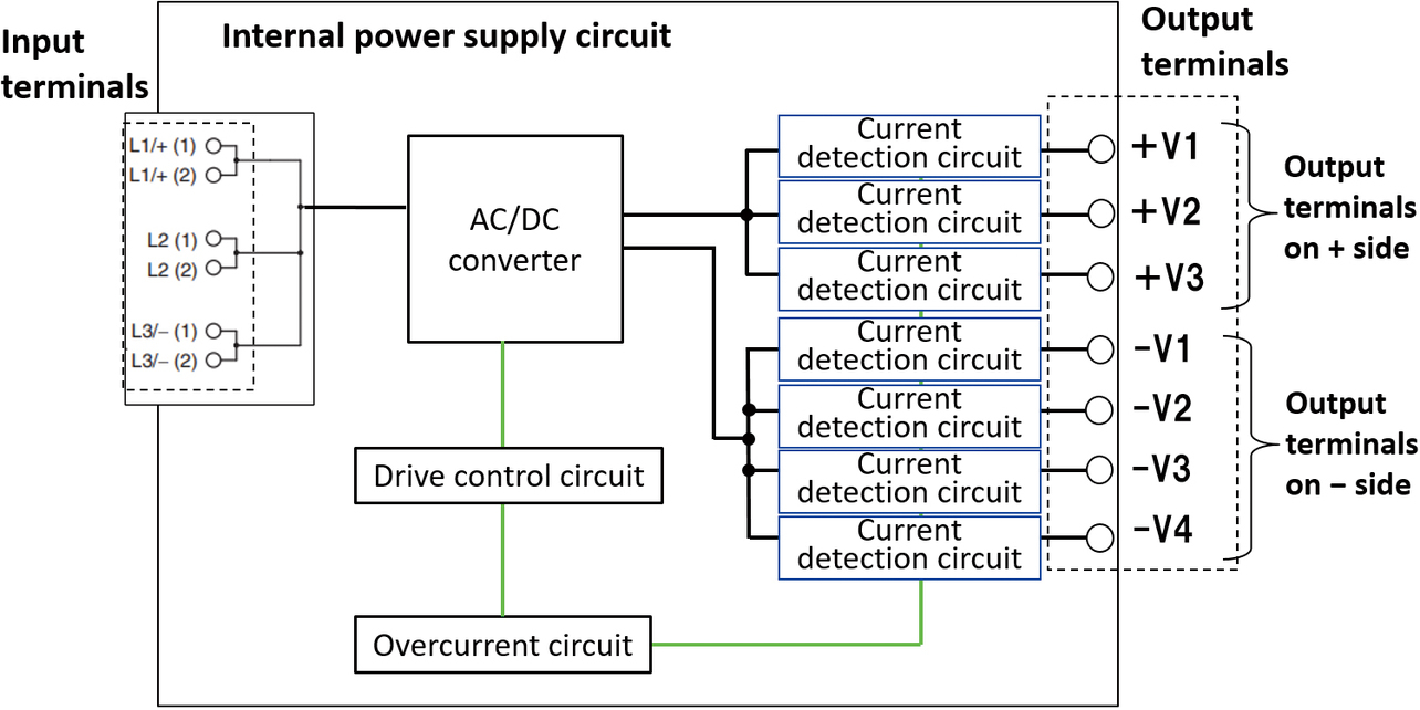
3.3 Terminal block overcurrent protection function for ensuring safety during faults
This subsection refers to Fig. 18 to explain the solution to the current flow concentration issue presented in Subsection 2.3. A power supply unit with a capacity of 2 kW can flow a current of approximately 85 A or more to the loads. We mounted a current detection circuit for each terminal block connecting to the power supply unit’s load line. We added a function that trips the protection circuit at the detection of a current of 45 A or more to reduce the output voltage and limit the current (terminal block overcurrent protection). Conventionally, a broken line would cause an unintended large current (85 A) to flow to a wire rated up to, for example, 45 A. By adding the abovementioned function to limit the maximum current to 45 A, we made it possible to avoid the risk of wire burnout even when thin wires are used.
However, when implementing this terminal block overcurrent protection function, we had a problem with the gap between the current required to be limited at each terminal block and the specification (target value). Table 5 shows a specific example. The problem was that the limited current value at the terminal block −V2 changed in response to a current flow to the other terminal block (terminal block −V1 in Table 5).
| Current flow to terminal block −V1 | Limited current value at terminal block −V2 | Gap with target value 45 A |
|---|---|---|
| 0 A | 45 A | N/A |
| 20 A | 44.4 A | −0.6 A |
| 40 A | 43.8 A | −1.2 A |
Fig. 19 illustrates the mechanism responsible for this phenomenon. Fig. 19 shows the circuit mounted on the negative side of the output terminals (−V1 to −V4) for terminal block overcurrent protection. The terminal block is shown as one with two poles (−V1 and −V2) for simplification. Rs1 and Rs2 represent current detection resistors, while ra, rb, and rc represent patterned resistance components.
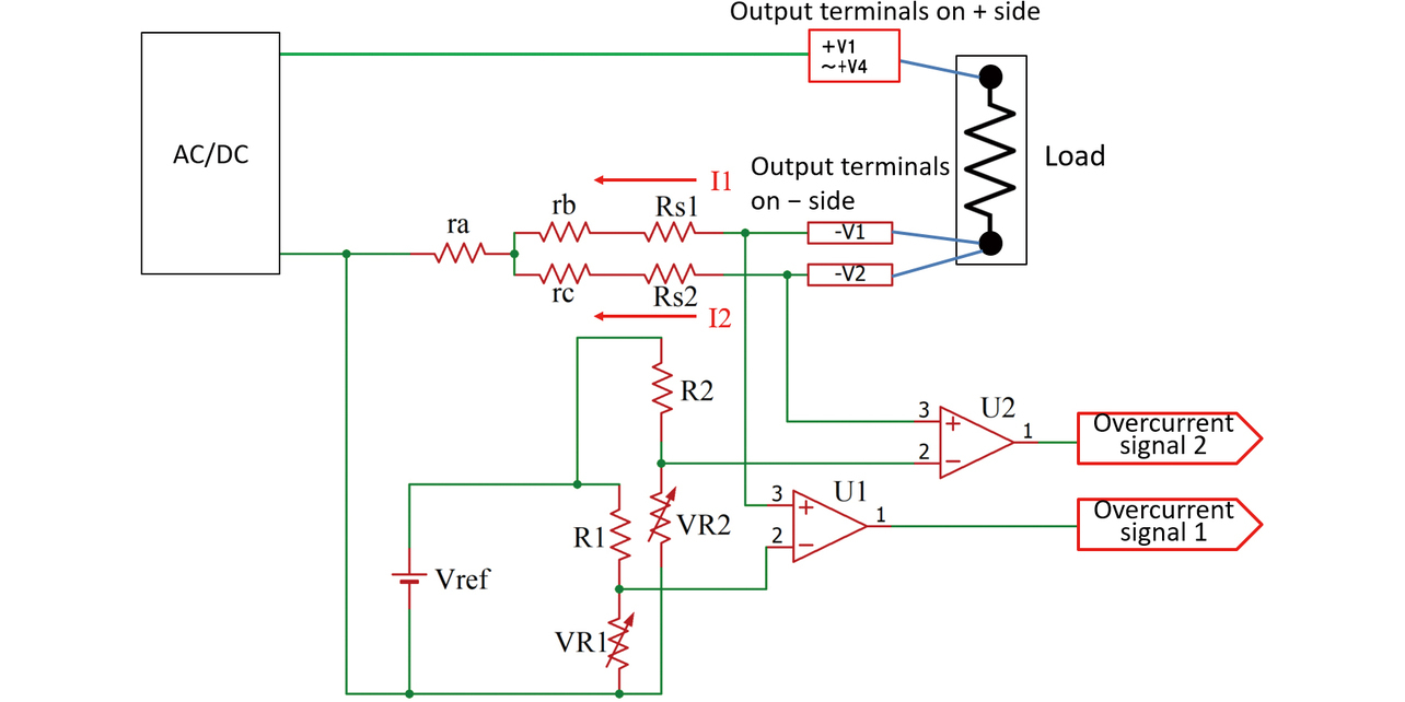
Let us take the −V2 terminal as an example. The terminal block overcurrent protection circuit normally detects the voltage that occurs in the sensing resistor (Vs2=Rs2×I2) due to a current flow. Then, this circuit sends an overcurrent signal to the control side if the detected voltage exceeds the reference voltage (operational amplifier’s V− voltage). However, the limited current at the terminal block −V2 is variable depending on the magnitude of the current flow (I1) to terminal block −V1. This variability is caused by the common impedance ra up to the sensing resistor. One can see that the limited current at the −V2 terminal is affected by I1, as expressed by the following equation:

It may be possible to reduce this common impedance ra by the ingenious arrangement or patterning of the sensing resistors. However, ra is challenging to eliminate completely.
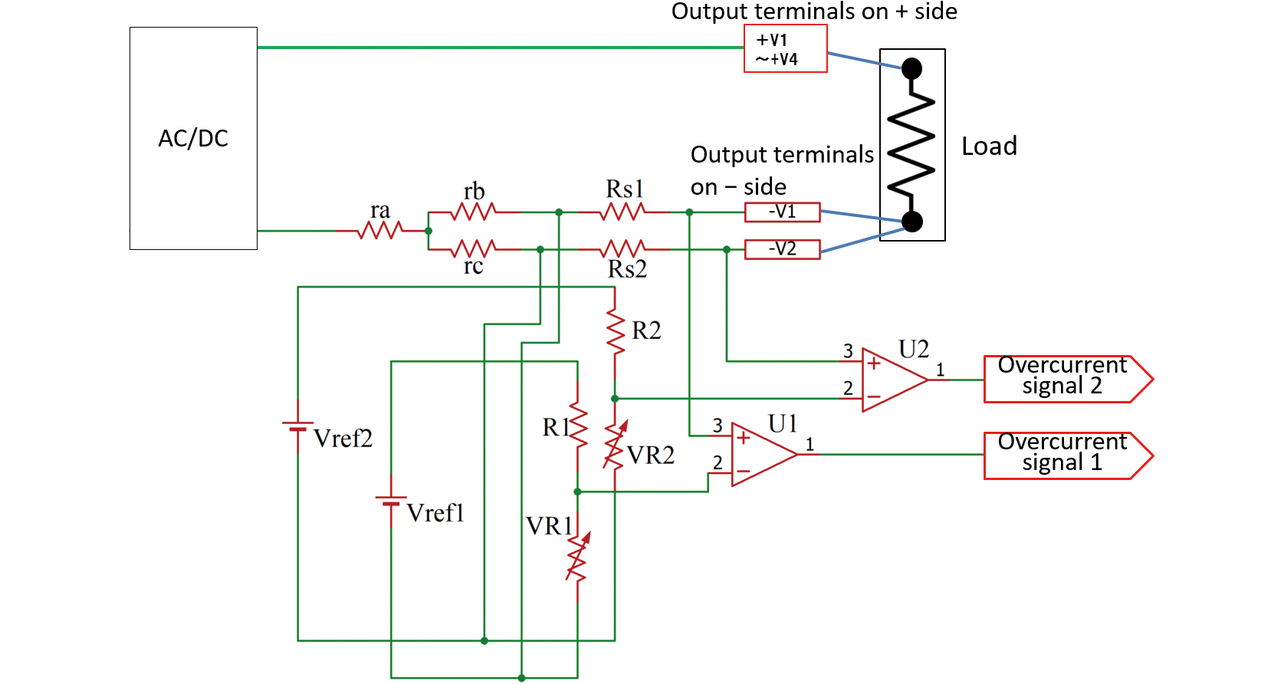
Then, to solve this problem, we created reference base voltages from around the sensing resistors Rs1 and Rs2, respectively, as in Fig. 20. As a result, the circuit became able to keep the limited current constant regardless of the presence or absence of a current flow to the other terminal. Thus, we successfully developed a sufficiently practical terminal block overcurrent protection function.
4. Conclusions
We explored a technology for developing a high-capacity power supply unit that could contribute to control panel miniaturization and GHG emissions reduction.
- We successfully enhanced the efficiency of our high-capacity power supply unit by adopting a primary series-secondary parallel LLC converter that could reduce loss by split current distribution over multiple elements. To start the design process, we identified the gain characteristic of this circuit system and determined the allowable ranges for the parameters for the current balance in the converter’s elements to fall within a target variation range of approximately 5%. As a result, a 2 kW power supply unit (Type S8VK-WA20224) achieved an efficiency of 95.4%, a significant improvement from the existing 1.5 kW power supply unit’s efficiency of 88.7%, and a decrease in size by 17%.
- We accurately calculated the losses in the transformers and other large magnetic components by a magnetic simulation to perform a thermal simulation with improved accuracy. This combined use of magnetic and thermal simulations enabled us to obtain an optimal heat dissipation structure and develop a compact high-capacity power supply unit with natural air cooling.
- We mounted a current detection circuit for each terminal block connecting to the load line and added a current-limiting function (terminal block overcurrent protection function). This function led us to successfully reduce the wire size and miniaturize the control panel by 10%.
Through these technical improvements, we developed a super-compact, low-loss 2 kW power supply unit, which successfully improved by 63% relative to the pre-existing product in terms of the GHG emissions from “Product Use” in the supply chain emissions (Scope 3, Category 11) (CO2 emissions FROM: 286 kg/year TO: 106 kg/year).
The market is seeking higher-capacity power supply units up-rated further to 3 kW or 4 kW. Our primary series-secondary parallel LLC converter may develop into variations with more transformers to adapt to such higher-capacity power supply units. Moving forward, we intend to pursue the converter design parameters for transformers’ optimal number and size to enable capacity-based miniaturization and efficiency enhancement.
References
- 1)
- E. Orietti et al., “Current sharing in three-phase LLC interleaved resonant converter,” in 2009 IEEE Energy Convers. Congr. Expo. 2009, pp. 1145-1152.
- 2)
- D. Huang, S. Ji, and F. C. Lee, “LLC Resonant Converter With Matrix Transformer,” IEEE Trans. Power Electron, vol. 29, no. 8, pp. 4339-4347, Aug, 2014.
- 3)
- J. Yuyang et al., “A DCX-LLC Resonant Converter with High Input-Output Voltage Ratio Based on an Integrated Matrix Transformer,” in IEEE Conf. Proc., 2022, vol. 2022, no. IECON, pp. 1-5.
- 4)
- Infineon Technologies. Resonant LLC Converter: Operation and Design. V1.0.(2012). Accessed: Oct. 1, 2023. [Online]. Available: https://www.infineon.com/dgdl/Application_Note_Resonant+LLC+Converter+Operation+and+Design_Infineon.pdf?fileId=db3a30433a047ba0013a4a60e3be64a1
The names of products in the text may be trademarks of each company.