


Partial Discharge Voltage Prediction in Printed Wiring Boards and Their Expansion to High Frequency
- Quality
- Partial Discharge
- Printed Wiring Board
- Power Electronics
- High Frequency
With the recent increase in the frequency and power of power conversion equipment, the risk of dielectric breakdown in multilayer printed wiring boards is increasing. In order to respond to risks, a technology for predicting the partial discharge generation site and partial discharge starting voltage, including support for the high frequency range, has been desired.
Conventionally, for simple shapes, such as twisted pairs of enameled wires and sphere electrodes, the partial discharge starting voltage has been predicted from electric field CAE analysis and theory. However, there was no predictive technology involving printed wiring boards, especially in the high-frequency region.
In this paper, assuming a multilayer printed wiring board, we investigated the prediction technique of partial discharge phenomena between the upper and lower copper traces with the insulating layer in between, especially in the high-frequency region (including the MHz band).
Clarification of the partial discharge starting voltage and discharge site by electric field CAE analysis and discharge theory, and the actual measurement evaluation showed that the partial discharge starting voltage in the high-frequency region can be derived by adding a frequency-dependent correction factor. As a result, it became possible to predict the partial discharge starting voltage up to 5 MHz with 30% accuracy.
1. Introduction
The approach to a decarbonized society is progressing toward the realization of carbon neutrality in 2050. In power conversion equipment, higher efficiency is required, and miniaturization (higher power density) that realizes decentralization toward the introduction of renewable energy is strongly required1).
On the other hand, in power semiconductors used for the switching of power conversion equipment, wide gap semiconductors (SiC, GaN, etc.) capable of higher voltage resistant and dealing with higher frequencies in comparison with conventional silicon (Si) are practicalized, and the environment where switching with higher frequencies (several hundred kHz–MHz) can be used is being realized. In addition, multilayer printed wiring boards are increasing, and the density of circuit pattern is becoming higher2,3). When the frequency of switching becomes higher, miniaturization of LC devices becomes possible, and further higher power density of power conversion equipment, in addition to the increase of multilayer printed wiring boards, can be realized.
However, higher power density of power conversion equipment by higher frequency and multilayer printed wiring boards causes an increase in surges and a reduction in insulation thickness, and, as a result, partial discharge is easily generated. Partial discharge means “discharge that only partially bridges insulation between conductors4).” Since the energy of a partial discharge is low and it slightly deteriorates the insulation layer, there arises no problem generally. However, since it is considered that the higher frequency of power conversion equipment accelerates the deterioration of the insulation layer by the partial discharge, the risk of dielectric breakdown becomes higher. On the other hand, the multilayer of printed wiring boards makes it difficult to estimate the discharge site, and the risk of dielectric breakdown becomes higher. Moreover, it is said that the frequency of the voltage application fluctuates the partial discharge starting voltage5), and the risk that the partial discharge is easily generated by a higher frequency is considered.
When planning measures for these risks, the building of technology for predicting the partial discharge generation site and the partial discharge starting voltage, including partial discharge behavior in high-frequency region, is effective.
For example, the identification of the partial discharge site by electric field CAE analysis (two-dimensional cross-section) using the shape of twisted pairs of enameled wire, the prediction of partial discharge starting voltage by the discharge theory (Paschen’s law), and experimental results are reported6). However, since it is not a three-dimensional shape like a printed wiring board and the applied voltage is targeted to impulse and low frequency, it is not an evaluation of high-frequency voltage.
In addition, the results of actual measurements in a simple shape (sphere electrode)7) and the evaluation of creep discharge of printed wiring boards8) are reported as the discharge evaluation of high-frequency voltage. However, the report concerning the partial discharge phenomenon between the upper and lower conductive patterns with the insulating layer (electric conductor) in between, especially the study that steps into the MHz region are hardly found.
Therefore, we assumed multilayer printed wiring boards and performed studies on technology for predicting partial discharge, including the high-frequency region between the upper and lower conductive patterns with the insulating layer in between. In this paper, we report that we estimated the partial discharge site and the partial discharge starting voltage by the three-dimensional electric field CAE analysis in the low-frequency region, then performed an actual measurement evaluation of frequency dependence of the partial discharge starting voltage and enabled correction of the partial discharge starting voltage in the high-frequency region.
2. Theoretical background
2.1 Partial voltage and discharge part in printed wiring board
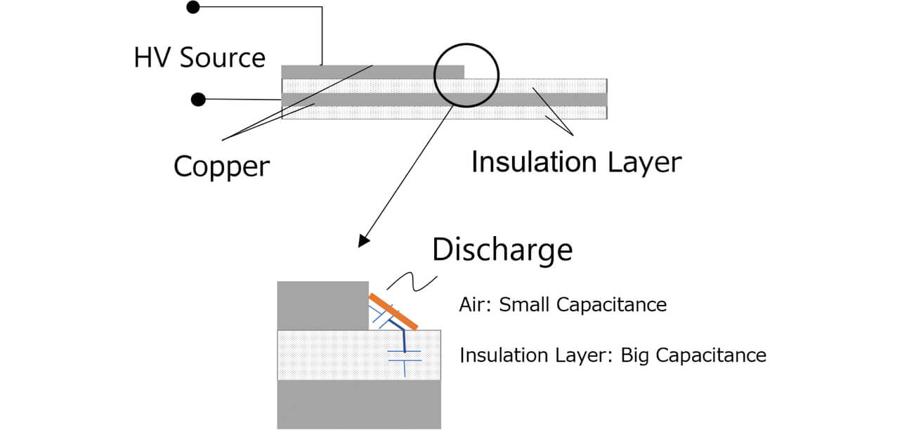
Partial discharge is defined as the discharge only partially bridging the insulation between conductors and does not include the discharge completely bridging between conductors (from JEC-0401-19904)). Since the discharge is mainly the movement of electrons associated with the dielectric breakdown of gas, the partial discharge phenomenon is generated in the gas part included between electrodes (between conductors). Since the discharge involves ozone generation and heat generation, the insulation layer close to the discharge will be deteriorated9).
An example of a partial discharge in a multilayer printed wiring board is shown in Fig. 1. In a multilayer printed wiring board, since the capacitance of the air part next to the copper trace and the capacitance of the insulation layer are arranged in series, voltage division enlarges the electric potential difference of the air part. In addition, since the discharge is mainly generated in the gas part, it can be assumed that the discharge is easily generated in the air part that is the gas part and in which the electric potential is large. Furthermore, the partial discharge starting voltage shall be the voltage value of the HV source in the discharge start of the printed wiring board.
2.2 Discharge generation condition (Paschen’s law)
Discharge reaches a continuous discharge in the following process. The first is the phenomenon (α action) that electrons accelerated between electrodes collide with gas atoms, ionize the atoms, and supply new electrons. The α action increases electrons exponentially, and insulation is broken down to perform the discharge. Since the cause of the α action is the collision of electrons and atoms, it is affected by the intermolecular distance suitable for acceleration until electrons have sufficient collision energy and collision probability (molecule density). In addition, the atoms that emitted the secondary electrons become ions, which collide with the electrode and supply electrons (γ action) to continue the discharge.
Discharge generation condition follows Paschen’s law10,11), (Fig. 2) which shows the discharge starting voltage becomes the function of the distance of the electrodes (d) applied with gas pressure (p)×voltage. The pd can be said to be similar to the density of gas molecules contained between electrodes and relates to the α action mentioned in the preceding paragraph. Although the curve varies depending on the type of gas, Fig. 2 shows the case of air. Fig. 2 shows that there exists the condition in which the discharge is most easily generated. When gas is air at normal temperature (25°C) and at 1 bar (1013.25 hPa), distance of electrodes of approx. 8 μm is the condition in which the discharge is most easily generated, and nearly 328 V is the discharge starting voltage. In addition, as shown by the state equation for gas, it should be noted that horizontal axis pd (density of gas molecule) is also affected by the ambient temperature.
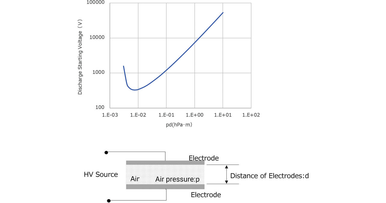
In addition, in the high-frequency region, it is known that the movement of ions with large mass affects the discharge starting voltage and changes Paschen’s law7,12). In the high-frequency region, the discharge start volage is said to become the function of the frequency (f) of the applied voltage×the distance of the electrodes (d) in addition to pd. For example, the actual measurement evaluation of the spherical electrode shows that the partial discharge starting voltage is reduced and is reduced to about 80% of DC at 1 MHz as frequency increases. On the contrary, the partial discharge starting voltage has a tendency to increase at 1 MHz or more7). This shows that the frequency of the applied voltage greatly changes the discharge starting voltage.
In printed wiring boards, since the change in the discharge voltage in the high-frequency region is unclear, we decided to obtain the theoretical formula for the experiment based on actual measurements.
As mentioned above, if we can evaluate the electric field distribution of the air part in a printed wiring board, it is possible to estimate the partial discharge starting voltage using the discharge condition of Paschen’s law (discharge starting voltage and pd), including the applied voltage frequency. (Furthermore, electric field distribution can be evaluated by electric field CAE as mentioned later.) Moreover, we considered that the acquisition of the frequency characteristic of the discharge starting voltage in printed wiring boards can predict the partial discharge starting voltage until the high-frequency region.
3. Studies of partial discharge starting voltage and discharge generation site by electric field CAE analysis and discharge theory
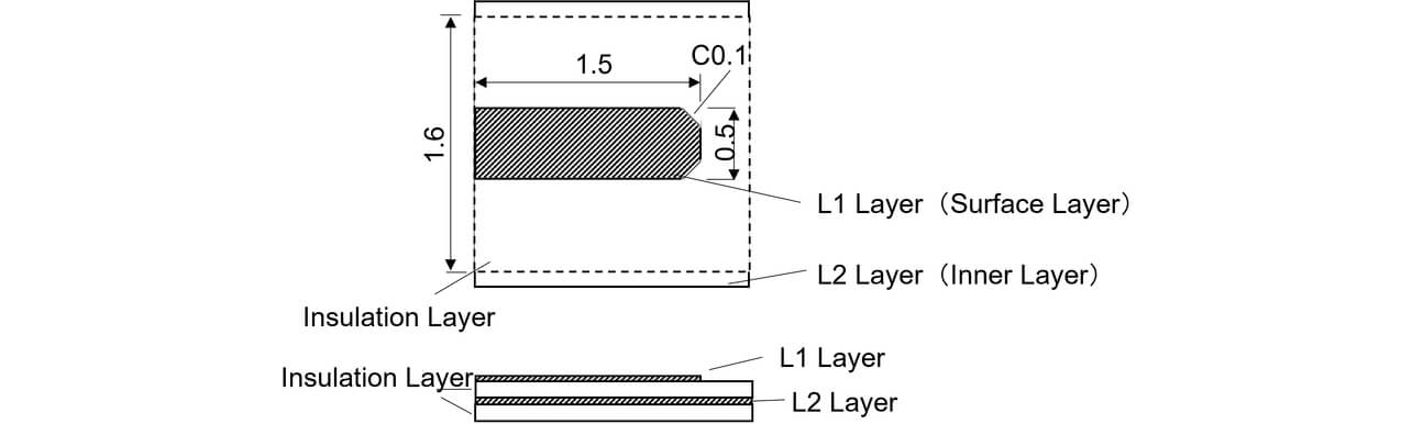
3.1 CAE study model
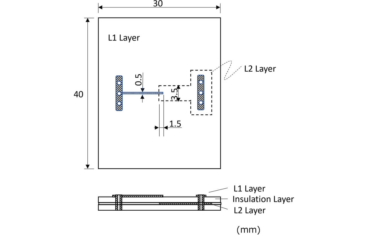
We created a study model for the CAE simulating multilayer printed wiring board as shown in Fig. 3. We assumed a general printed wiring board having L1 and L2 layers made of copper and with thickness of 18 μm. Insulation layers are also based on those (FR4 prepreg thickness) of a general printed wiring board and consist of four types of 0.076 mm, 0.1 mm, 0.15 mm, and 0.3 mm. In addition, the material constants used are shown in Table 1. Since specific dielectric constant and dielectric loss tangent of FR4 hardly change until reaching the MHz band, we used fixed values. Furthermore, the corner of the L1 layer was chamfered to 0.1 mm considering the etching accuracy of the printed wiring board.
| Layer | Material | Material constants | ||
|---|---|---|---|---|
| Conductivity (S/m) | Specific dielectric constant | Dielectric loss tangent | ||
| L1/L2 layers | Cu | 5.98E7 | — | — |
| Insulation layer | FR4 | — | 4.25 | 0.01 |
3.2 Analysis condition for electric field CAE
FEMTET (Murata Software) was used for the electric field CAE analysis. In addition, we performed the analysis by applying AC voltage between the L1 and L2 layers as shown in Fig. 4. We set the frequencies of 5 MHz and current of AC 60 Hz and 300 kHz, which is almost midway between them as the high-frequency region that is predicted in power electronic devices in the future.

3.3 Method for determining partial discharge in electric field CAE analysis
The results of the electric field CAE analysis in the applied voltage of AC 1 kV0-P and frequency of 60 Hz (electric field contour diagram for surface of insulation layer) are shown in Fig. 5, which shows that the electric field concentrates at the chamfered edges of L1 layer. It is anticipated that the discharge is generated in this position theoretically.
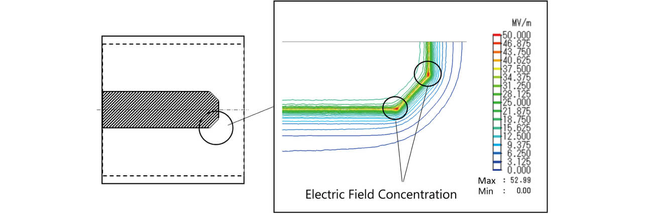
As afore mentioned, the condition in which the discharge is most easily generated according to Paschen’s law is that the electrode distance was approx. 8 μm and the potential difference was 328 V at normal temperature and normal pressure (25°C and 1 bar = 1013.25 hPa). In the printed wiring board this time, the air layer between the L1 layer and the insulation layer performs the discharge. Therefore, the partial discharge starting voltage in the electric field CAE analysis was introduced as follows. The space distance between the L1 layer and the insulation layer of 8 μm and the place where the potential difference is the largest (electric field concentration place in Fig. 5) are found from the results of electric field CAE under a certain applied voltage, and the applied voltage is changed so that the potential difference in the electric field concentration place is 328 V. The applied voltage at that time was assumed to be the partial discharge starting voltage. In addition, the temperature (135°C) at highland (3,000 m above sea level) and close to the hot electronic component was assumed from the standard of the power control equipment. In this case, when simply converting at a density ratio to 25°C, atmospheric pressure is calculated to be 518.60 hPa. When converting this according to Paschen’s law, the discharge conditions are the space distance of 15.6 μm and 328 V.
Furthermore, the influence of the frequency characteristics in Paschen’s law was not added to this electric field CAE analysis. Only the change in the electric field distribution by frequency was considered.
3.4 Analysis results
Fig. 6 shows the results of the electric field CAE analysis. The partial discharge starting voltage was described based on the peak value of the voltage (V0-P). The result shows that the increase in the insulating layer thickness heightens the partial discharge voltage. In the condition of 518.60 hPa, the partial discharge starting voltage is reduced by about 30% in comparison with that at normal temperature and normal pressure (1013.25 hPa).
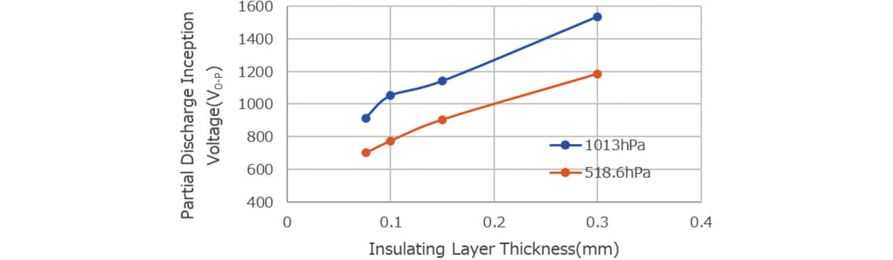
This is because when atmospheric pressure changes from 1013.25 hPa to 518.60 hPa, the space distance in which discharge starting voltage is the lowest value becomes larger from 8 μm to 15.6 μm. When space distance is larger, the discharge becomes easier because the potential difference becomes greater (in case of the same electric field distribution). This result suggests that the insulation design for power conversion equipment in the highland and in a hot environment should be performed carefully.
Furthermore, the electric field distribution hardly changed in the frequency region studied this time. Therefore, in this electric field CAE analysis, the partial discharge starting voltage has no frequency dependence.
4. Experiment of frequency influence on partial discharge starting voltage
4.1 Experiment sample and experiment condition
We studied the frequency influence by actually measuring the partial discharge starting voltage until reaching the high-frequency region in printed wiring boards. Multilayer printed wiring boards where the thickness of the insulation layer were prepared as shown in Fig. 7 and Table 2. Dimensions and material characteristics were made equivalent to those of electric field CAE. Furthermore, although the insulation layer is FR4, the material where the dielectric constant is prescribed was used.
| Layer | Material | Thickness (mm) |
|---|---|---|
| L1/L2 layers | Cu | 0.035 |
| Insulation layer | FR4 (Dielectric constant 4.2-4.4) | 0.076, 0.1, 0.15 and 0.3 |
In addition, in order to measure partial discharge behavior in the high-frequency region, AC voltages at 20 kHz, 300 kHz, 1 MHz, 2 MHz, and 5 MHz were applied between the L1 and L2 layers to conduct the experiments.
Moreover, 135°C and an altitude of 3,000 m were converted atmospherically, and the comparison with normal temperature and normal pressure was performed. Specifically, atmospheric pressure was adjusted to 518.60 hPa and 1013.25 hPa at ambient temperature of around 25°C to conduct the experiments.
4.2 Evaluation system for partial discharge
Evaluation of partial discharge was performed by applying AC voltage to samples in a shield room using the system as shown in Fig. 8 (shield room used to conform to Radio Law, and shield tent used for human body protection). Different configurations were adopted for 20–500 kHz and 1–5 MHz due to the limitation of amplifier frequency. Components used are shown in Table 3.
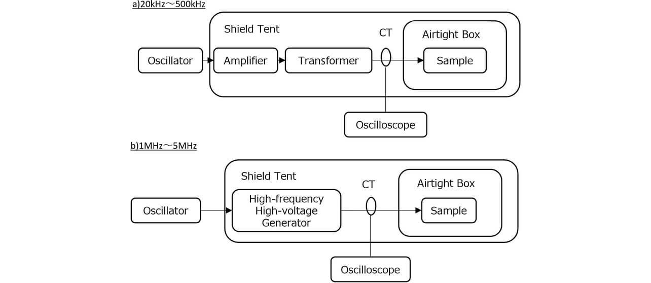
| Component | Manufacturer and model |
|---|---|
| Oscillator | Tektronix, Inc. AFG1022 |
| High-frequency amplifier | NF Corporation HSA4052 |
| Transformer | Two types for 20 kHz and 300–500 kHz (Our own making) |
| Oscilloscope | Tektronix, Inc. MSO44-3-BW-500 |
| High-frequency high-voltage generator | Customized product |
In addition, CT for the high frequency of our own making was used for measurement of the partial discharge, and high-frequency current generated by the discharge was acquired. Furthermore, experiments were conducted by using an airtight box and adjusting the atmospheric pressure.
4.3 Method for evaluating partial discharge
The CT current waveform with and without partial discharge generation is shown in Fig. 9, which shows the waveform like noise appears when the partial discharge is generated. Applied voltage when this waveform is generated was assumed to be the partial discharge starting voltage.
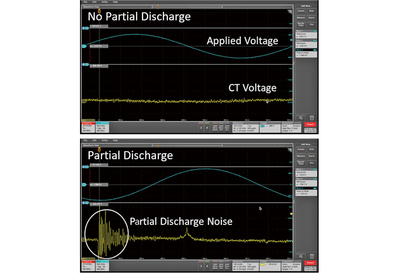
Furthermore, voltage application time was assumed to be 10 sec, which is sufficient for judging partial discharge generation in this experiment. When no generation of the partial discharge is found for 10 sec, we raised the applied voltage by 20 V for remeasurement and repeated this until generation of the partial discharge.
4.4 Method for observing partial discharge
UV camera (ViewTer-500UV 3R Co.) was used for the observation of UV light emitted from the partial discharge.
5. Results of experiment for influence of frequency on partial discharge starting voltage
5.1 Dependence of partial discharge starting voltage on atmospheric pressure and frequency
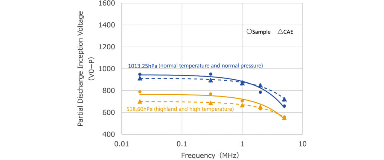
Experiment results when changing applied frequency and thickness of the insulation layer are shown in Figs. 10 and 11. Atmospheric pressure is different in Figs. 10 and 11.
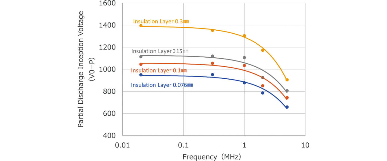
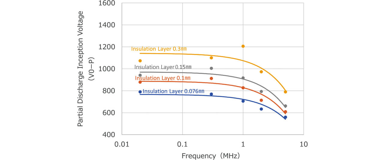
From the comparison of Figs. 10 and 11, we found that when atmospheric pressure is reduced (highland and high temperature), the partial discharge starting voltage was uniformly reduced by about 20% without relating to frequency. We estimate that this is because atmospheric and frequency influence the partial discharge starting voltage and have little interaction in Paschen’s law.
Furthermore, there is a tendency that the partial discharge starting voltage is linearly reduced associated with the increase in the frequency without relating to the thickness of the insulation layer and atmospheric pressure (reduction ratio is about 0.7% per 100 kHz). Since this is considered to be frequency dependence in Paschen’s law, it is adopted as the correction factor for the discharge starting voltage.
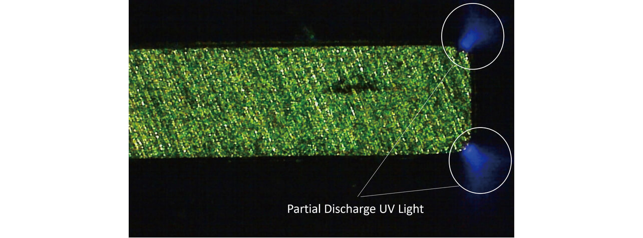
5.2 Position of partial discharge generation
We performed the observation of UV light emitted by the partial discharge. Fig. 12 shows a photograph of the partial discharge at the corners of the L1 layer of an experiment sample and allows observation of the generation of the partial discharge in a position the same as the electric field concentration by electric field CAE (see Fig. 5).
5.3 Dielectric breakdown by partial discharge in MHz band
The partial discharge starting voltage was continuously applied to a sample with an insulation layer thickness of 0.076 mm at 1 MHz. As a result, dielectric breakdown occurred in about 100 sec. Thereafter, the surface of the printed wiring board after the dielectric breakdown was observed. The observation result is shown in Fig. 13, which shows that the FR4 part has holes in the place of the partial discharge generation.
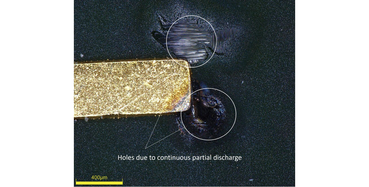
At high frequencies like 1 MHz, the sample easily reached dielectric breakdown within 100 sec only by partial discharge.
6. Reflection of frequency characteristic to electric field CAE analysis
From the experiment results, the following matters were found in Paschen’s law considering printed wiring boards. (i) Atmospheric pressure and frequency are independent. (ii) The discharge starting voltage is a linear function of frequency (reduced by about 0.7% per 100 kHz). From these, we presumed that Paschen’s law, including up to the high-frequency region, can be calculated by adding the correction factor dependent on the frequency (up to 5 MHz). Therefore, we estimated the partial discharge starting voltage based on the electric field CAE analysis and Paschen’s law added to the influence of frequency. An example of an insulation layer thickness of 0.076 mm is shown in Fig. 14.
Qualitative tendencies of estimated and measured values by CAE coincide. Since the maximum error is about 30%, including other insulation layer thicknesses, the prediction of the partial discharge starting voltage can be said to be possible. As one of the causes of errors on the low-frequency side, the shape accuracy of experiment samples can be listed. Since the Cu trace shape of printed wiring boards is created by etching, the surface has microscopic unevenness. In addition, the insulation layer also has unevenness. Therefore, we presume that the change in electric field distribution causes the difference in the estimated and measured values.
7. Discussion
In printed wiring boards where experiment evaluations were performed this time, the partial discharge starting voltage was linearly reduced (down to 5 MHz) as frequency increased. In the afore-mentioned spherical electrode, the partial discharge starting voltage was reduced down to about 1 MHz, and thereafter turned to an increase. We will discuss this difference.
Ionization of atoms is related to the afore-mentioned discharge. When high-frequency AC voltage is applied to an electrode, a part of the ions with large mass ionized by the α action is trapped because it cannot follow the fluctuations of the electric field. Therefore, the electric field between the electrodes is greatly distorted even with voltage the same as low frequency, and the potential difference is locally enlarged. As a result, the discharge starting voltage is reduced at a high frequency. In addition, at higher frequencies, many ions are trapped between electrodes, the γ action is deactivated, and the discharge starting voltage rises7,12).
Since the above phenomenon is the movement of ions in a uniform electric field, it is greatly affected by the condition of the distance between the electrodes and the electric field.
Since the electric field between the spherical electrodes is uniform, movement is considered to be close to the theoretical one. On the other hand, in printed wiring boards, non-uniform electric fields exist between the Cu trace and the insulation layer, and the movement of ions is considered to be different in each place. Therefore, we estimate that the dependence of the partial discharge starting voltage on frequency in spherical electrodes and printed wiring boards is different.
8. Conclusions
Higher frequency and higher power of power conversion equipment in recent years increases the dielectric breakdown of multilayer printed wiring boards. To deal with this risk, technology for predicting partial discharge generation sites and the partial discharge starting voltage, including the risk in high-frequency regions, was required.
Conventionally, although there was an attempt to predict the partial discharge starting voltage from electric field CAE analysis and theory for simple shapes, such as twisted pairs and spherical electrodes, there was no prediction technique involving printed wiring boards, especially including the high-frequency region.
In this paper, assuming a multilayer printed wiring board, we investigated the prediction technique of partial discharge phenomena between the upper and lower copper traces with the insulating layer in between, especially in the high-frequency region (including the MHz band).
As a result of the investigation, the partial discharge starting voltage and discharge site were clarified by electric field CAE analysis, and a correction factor up to high-frequency region was introduced to enable prediction of the partial discharge starting voltage up to 5 MHz. In addition, we found that dielectric breakdown occurs in short time at high frequencies.
This investigation was able to identify the quality risk associated with the higher power density of power conversion equipment.
In addition, we are going hereinafter perform a comparison with other pattern shapes and the improvement of prediction accuracy, including creep discharge.
The Quality Engineering Section is establishing the design criteria for multilayer printed wiring boards for power electronic products. This section is performing studies of product trends and precedent quality risks based on technical trends and will perform the activities continuously in the future.
References
- 1)
- Ministry of Economy, Trade and Industry, “Green Growth Strategy Associated with Carbon Neutral in 2050,” Website of Ministry of Economy, Trade and Industry, Sep. 3, 2021, https://www.meti.go.jp/policy/energy_environment/global_warming/ggs/index.html (accessed Jan. 20, 2023).
- 2)
- Y. Takahashi and T. Endoh, “The Latest Power Device and Power Electronic Integration Technology,” J. Jpn. Inst. Electron. Packag., vol. 24, no. 3, pp. 215-225, 2021.
- 3)
- Electronic Parts and Packaging Technology Committee, “Current and Future Prospects in Packaging Technology,” J. Jpn. Inst. Electron. Packag., vol. 22, no. 1, pp. 28-32, 2019.
- 4)
- Partial discharge measurement, JEC-0401, The Institute of Electrical Engineers of Japan, 1990.
- 5)
- Y. Okamoto, “Fundamentals of Process Plasma,” J. Vac. Soc. Jpn., vol. 59, no. 7, pp. 161-170, 2016.
- 6)
- D. Muto, Y. Ikeda, K. Tomizawa, H. Fukuda, M. Kozaka, and M. Hikita, “Partial Discharge Characteristics of Winding Applied with Enameled Film with Air Bubble,” Furukawa Electric Rev., vol. 138, pp. 46-53, 2019.
- 7)
- Discharge Handbook Publication Committee of The Institute of Electrical Engineers of Japan, Eds., Discharge Handbook Part 1. 3rd ed., Tokyo, Ohmsha, 2003, 529p., ISBN4-88688-308-6.
- 8)
- Safety requirements for power electronic converter systems and equipment–Part 1: General, JIS C 62477-1 Appendix F, Japanese Industrial Standard, 2017.
- 9)
- N. Izeki, “Corona Resistance and Ozone Resistance of Polymer Structure,” High polymers, Japan, vol. 10, no. 8, pp. 693-697, 692, 1961.
- 10)
- T. Kaneda, Gas Electronics, 1st ed., Tokyo, Corona Publishing, 2003, 226p., ISBN4-339-00745-5.
- 11)
- O. Yamamoto and S. Hamada, High Voltage Engineering. 1st ed., Tokyo, Ohmsha, 2013, 235p., ISBN978-4-274-21444-8.
- 12)
- S. Takeda, Fundamentals of Gas Discharge, 2nd ed., Tokyo, Tomeisha, 1975, 185p.
AICOT® is a trademark of OMRON Corporation.
The names of products in the text may be trademarks of each company.