


Novel GaN Device Gate Drive Technique for High Efficiency and Noise Reduction
- Power Electronics
- Wide Gap Semiconductor
- Gate Drive Circuit
- Spike gate voltage
- High Frequency
Recently, high-speed switching circuits using GaN GIT have attracted attention for higher power density. In particular, GaN GIT devices have an ultrafast speed capability but tend to cause false turn-ons due to a lower threshold voltage. A simple RC-type gate drive method is usually used to prevent the false turn-on phenomenon. However, during the turn-off period, the spike gate voltage will exceed the rated voltage, it is necessary to slow down the turn-off switching speed, and the high-speed switching characteristics of GaN GIT could not be fully utilized. To solve this problem, we propose a novel GaN GIT gate drive technique using a two-step turn-off method. It is possible to simultaneously satisfy the conflicting performance of low spike voltage and high speed turn-off switching. This circuit was implemented on the board using the GaN GIT device and applied to a synchronous rectification type boost converter. It is confirmed experimentally that this drive technique is verified as useful.
1. Introduction
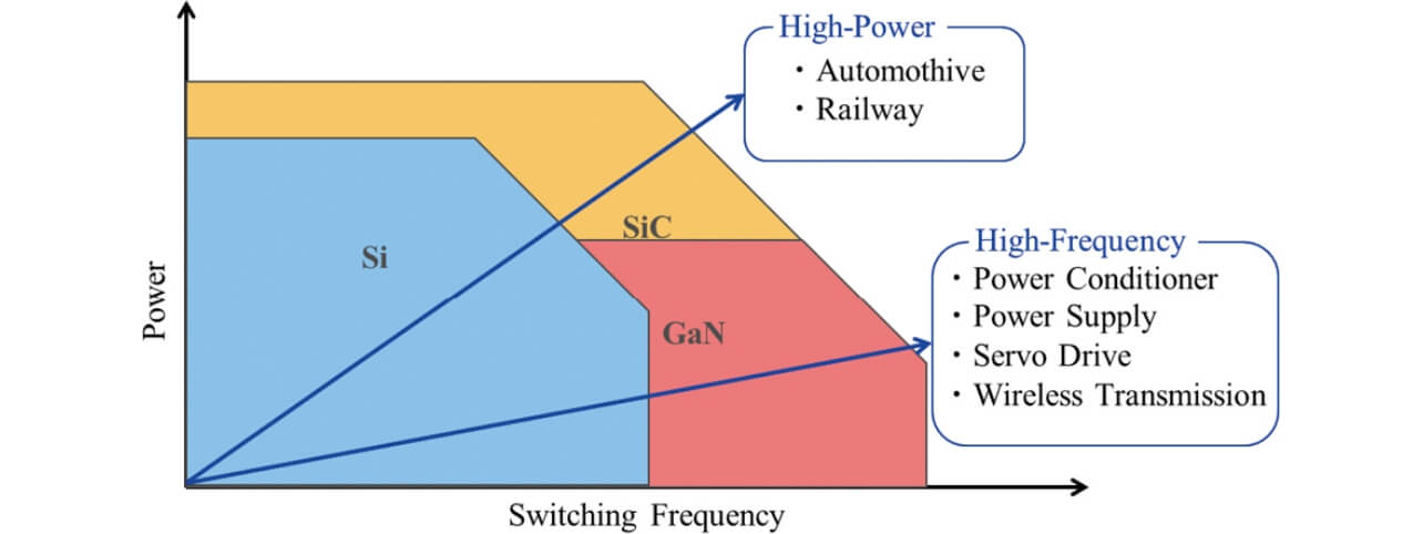
In recent years, wide gap semiconductors have attracted attention as the material for new semiconductor devices in place of silicon (Si) toward the realization of higher power density and higher efficiency of power converters1). The power converter is mostly occupied by cooling parts (heat sink) and passive parts (capacitor and reactor), and higher efficiency and higher frequency can realize size and cost reductions of these parts. The power converter (power conditioner, multipurpose power supply, and servo drive) as one of the product groups of OMRON is for power of several hundred W to several kW, and especially we study the application of gallium nitride (GaN) as shown in Fig. 1. The Si device has the large input and output capacitance and the poor reverse recovery operation of a body diode, while the GaN device has capacitance far lower than the former and is excellent in the reverse recovery characteristic. Therefore, the use of the GaN device can realize higher efficiency. In order to derive the material characteristic of the GaN device to the limit, the GaN devices with various internal structures, such as the vertical structure2) and the horizontal structure3) have been developed. The depression mode4) GaN is a normally-on device, and the enhancement mode (E-M)5) GaN realizes an easily handled, normally-off device. In addition, the hybrid mode (H-M)6) structure using MOSFET has been also developed. Table 1 shows the comparison of parameters of available typical devices. Here blue and red letters show the advantages and disadvantages, respectively. GaN GIT (gate injection transistor)7) attracts attention as a device of which normally-off action and capacitance C and electric charge Q are low as shown in Table 1 and which can realize high speed drives.
| Si | SiC | GaN H-M |
GaN E-M |
GaN GIT |
|
|---|---|---|---|---|---|
| Vds [V] | 600 | 650 | 650 | 650 | 600 |
| Id [A] Max. | 35 | 39 | 34 | 30 | 31 |
| Rdson [mΩ] Typ. | 52 | 48 | 50 | 50 | 55 |
| Ciss [pF] Typ. | 2850 | 1118 | 1000 | 242 | 380 |
| Co (tr) [pF] Typ. | 1050 | 194 | 310 | 160 | 102 |
| Qg [nC] Typ. | 68 | 33 | 16 | 6.1 | 5.8 |
| Qoss [nC] Typ. | ― | 78 | 126 | 64 | 41 |
| Qrr [nC] Typ. | 6000 | 125 | 126 | 0 | 0 |
| Vth [V] Typ. | 3.5 | 4.5 | 4 | 1.7 | 1.2 |
This paper explains focusing on GaN GIT. The threshold voltage Vth of this device is far lower than that of the Si device as shown in Table 1, and it is very important to maintain the off state for GaN GIT. GaN GIT is sensitive to noise, and negative gate voltage is required for the prevention of the incorrect turn-on of GaN GIT by the miller current. When incorrect turn-on occurred because of the absence of negative gate voltage, the arm short-circuit phenomenon may occur, leading to catastrophic failure. The negative gate voltage is normally implemented by the bipolar power supply. In order to derive the switching performance of GaN GIT, the RC type gate drive method8,9,10,11) proposed. Since this method can drive the gate of GaN GIT in higher voltage, high speed switching can be realized. However, the high-speed property of the turn-off generates high negative spike gate voltage.
In order to solve these problems, we propose the GaN GIT gate drive method of two-step turn-off that can simultaneously realize the contrary performance of low noise and a high-speed turn-off switching. Chapters 2 and 3 will explain the operation principle of the conventional gate drive circuit and the proposed gate drive circuit. Chapter 4 applied the proposed gate drive circuit to the synchronous rectification type DC/DC converter to verify the effectiveness experimentally.
2. Conventional gate drive circuit
2.1 Circuit structure
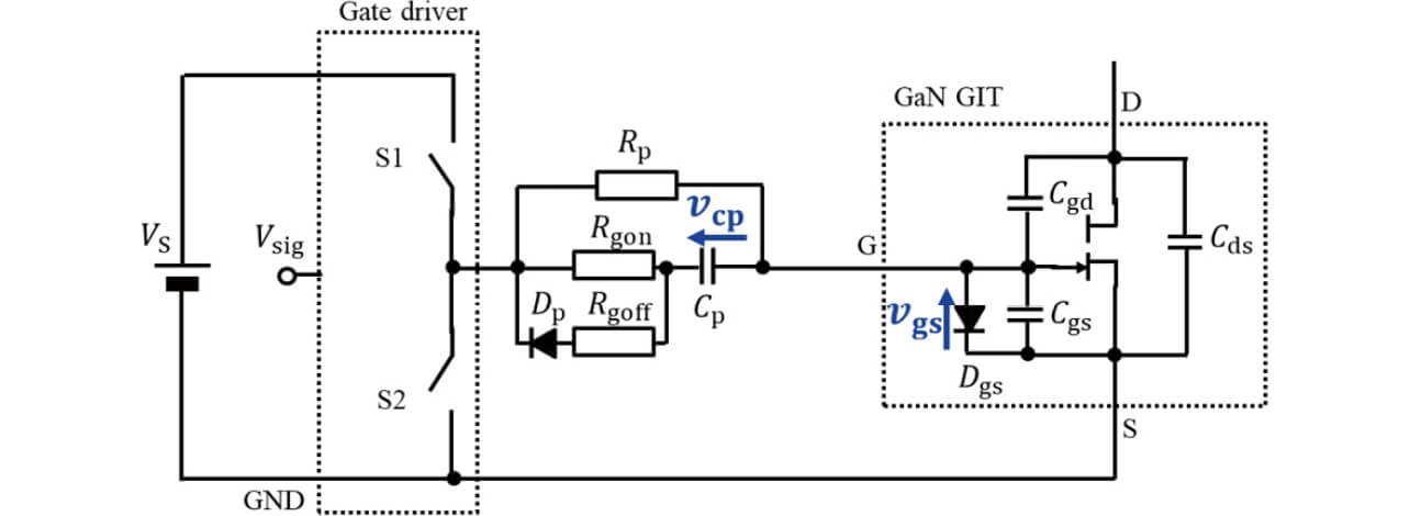
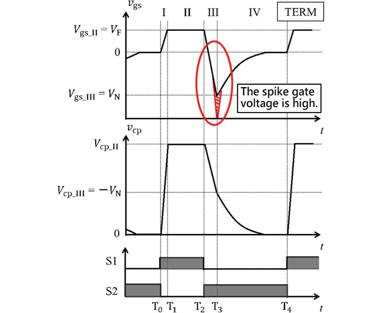
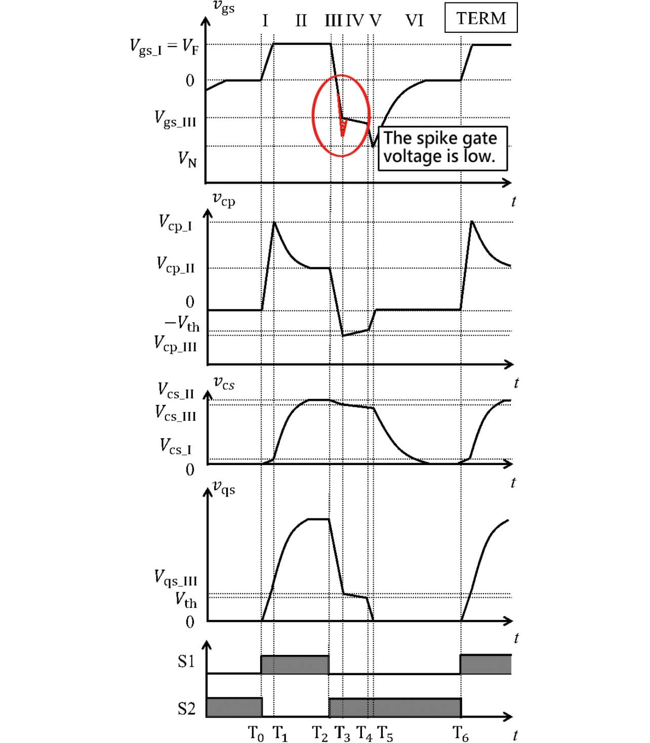
Fig. 2 shows the structure of the conventional RC type gate drive circuit. Although this circuit is simple and has been actually used for many years, the high negative spike gate voltage may be caused during the higher speed turn-off as shown in Fig. 3 (part encircled by the red line). Therefore, it hinders high frequency switching.
2.2 Operation principle
Fig. 3 shows the operation sequence. Fig. 4 shows the equivalent circuit in each period of the conventional RC type gate drive circuit. Concerning Fig. 3, since the resistances Rgon and Rgoff are very small, the operation principle will be explained neglecting these.
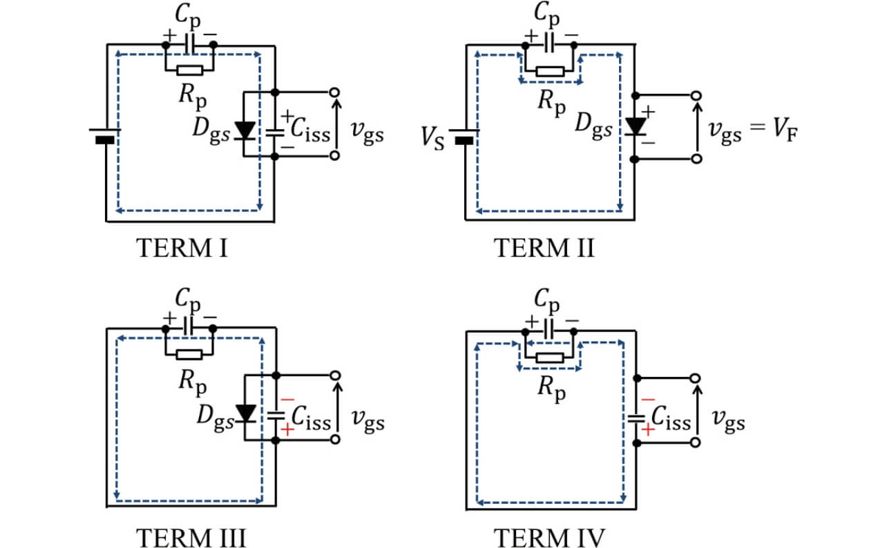
TERM Ⅰ [ ]:
]:
When switch S1 is turned on at T0, the input capacitance (Ciss = Cgs + Cgd ) of GaN GIT starts charging through the capacitance CP. Simultaneously, the electric current starts to flow in the parasitic diode Dgs formed between the gate and the source of GaN GIT.
TERM Ⅱ [ ]:
]:
When turn-on is completed, the gate current always flows through RP to the parasitic diode between the gate and the source to maintain the turn-on condition. vgs is clamped by the forward voltage (VF) of the parasitic diode. This depends on the band gap of GaN GIT. The gate resistance RP is generally designed so that VF of the parasitic diode is approximately 3.5 V. Voltages Vgs_Ⅱ and VCP_Ⅱ in the period II are given by the equations (1) and (2), where VS is the gate supply voltage.


TERM Ⅲ [ ]:
]:
When switch S2 is turned on at T2, the capacitance Ciss starts discharging through the capacitance CP. vgs decreases corresponding to that. Negative voltage VN can be calculated using the general MOSFET equation (3)12), where Qg is the total gate electric charge from 0 V to VF. Switching speed can be adjusted by the resistance Rgoff. Since the gate voltage sharply changes to negative, the high spike gate voltage is additionally generated in VN.

TERM Ⅳ [ ]:
]:
The capacitances Ciss and CP are discharged through the resistance RP. The gate voltage vgs approaches 0 V in the above RC time constant. vgs_Ⅳ voltage during the period Ⅳ is given by the equation (4).
![vgs_Ⅳ(t)=VN・exp[-(t-T3)/RP(CP+Ciss)]](/global/en/assets/img/technology/omrontechnics/vol53/015/img_04.svg)
3. Proposed gate drive circuit
3.1 Circuit structure
Fig. 5 shows the gate drive circuit of the two-step turn-off constituted by QS, RS, and CS (part surrounded by red dotted line). The active miller clamp MOSFET QS used for preventing the incorrect turn-on of a power transistor caused by the miller current is implemented in a commercialized gate driver.
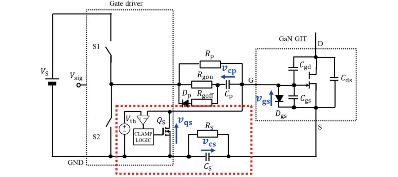
When the miller clamp function is used, the gate voltage of the power transistor is generally clamped at approximately less than 2 V in the off condition. The proposed gate drive circuit can reduce the spike gate voltage during turn-off as shown in Fig. 6 (encircled in red).
3.2 Operation principle
Fig. 6 shows the operation sequence. Fig. 7 shows the equivalent circuits of the proposed gate drive circuit in each period. Concerning Fig. 7, the resistances Rgon, Rgoff, and the capacitance of MOSFET QS are neglected because they are so small. It is assumed that the capacitance CP is much smaller than the capacitance CS.
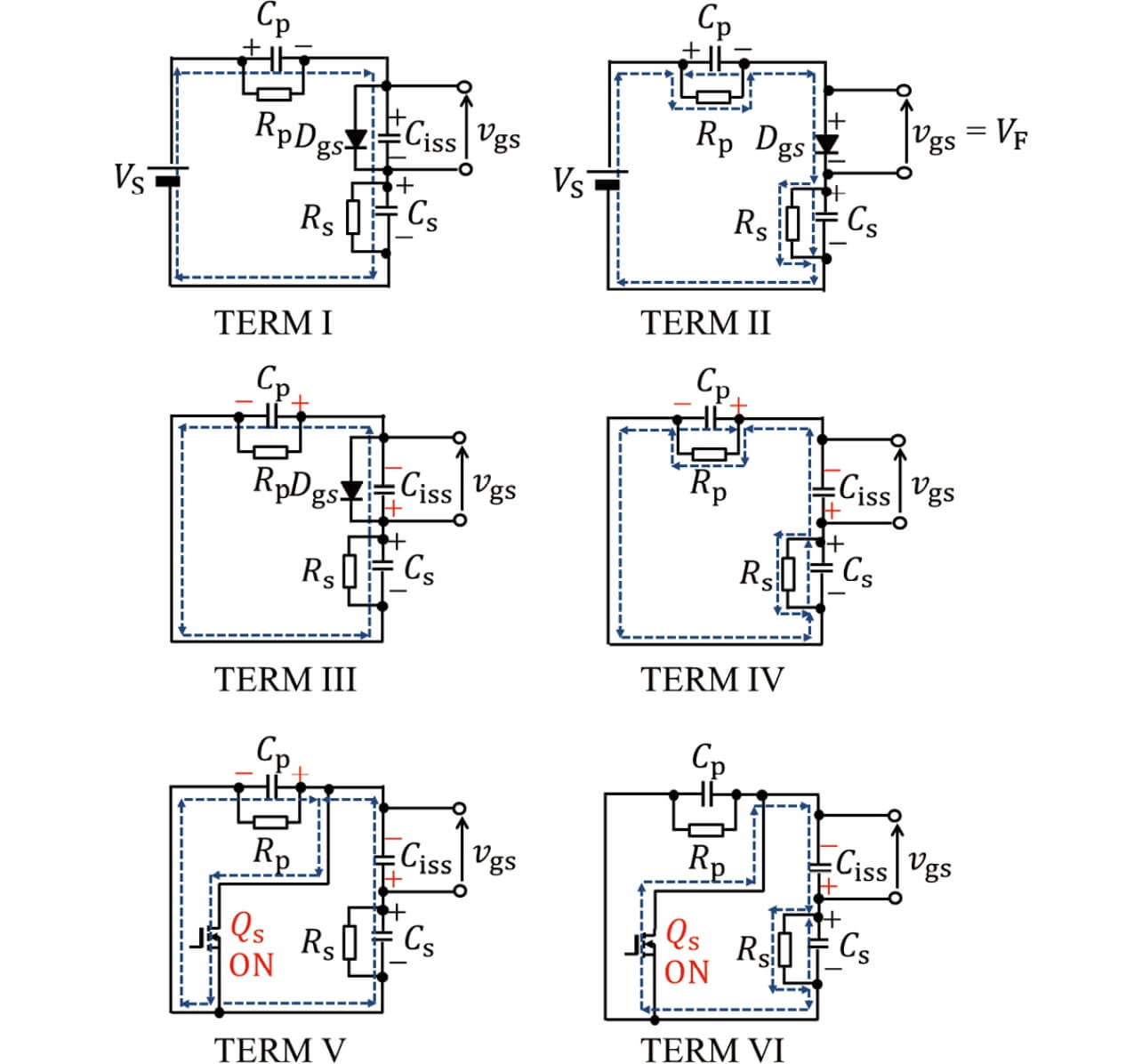
TERM Ⅰ []:
Switch S1 is turned on at T0, the input capacitance (Ciss) of GaN GIT starts charging through the capacitances CP and CS. Vgs_Ⅰ, VCP_Ⅰ, and VCS_Ⅰ voltages at the end of the period Ⅰ are shown in equations (5), (6), and (7).


TERM Ⅱ []:
When turn-on is completed at T1, vgs is clamped by the forward voltage (VF) of the parasitic diode Dgs. The capacitances CP and CS are discharged and charged through the resistances RP and RS. VCP_Ⅱ and VCS_Ⅱ voltages at the end of the period II are expressed by equations (8) and (9) using the general equation12) of MOSFET.
![VCP_Ⅱ=VCP_Ⅰ(1-CP+CS/CS RP/RP+RS)・exp[-(T2-T1)/(RP・RS/RP+RS)(CP+CS)]+(VS-VF)RP/RP+RS](/global/en/assets/img/technology/omrontechnics/vol53/015/img_08.svg)
![VCS_Ⅱ=VCS_Ⅰ(CP+CS/CP RS/RP+RS-1)[1-exp[-(T2-T1)/(RP・RS/RP+RS)(CP+CS)]]+VCS_Ⅰ](/global/en/assets/img/technology/omrontechnics/vol53/015/img_09.svg)
TERM Ⅲ []:
When switch S2 is turned on at T2, the capacitance Ciss of the GaN GIT starts charging through the capacitances CP and CS. When the electric charge of each capacitor is balanced, the discharge ends. Vgs_Ⅲ, VCP_Ⅲ, VCS_Ⅲ, and Vqs_Ⅲ voltages at the end of the period Ⅲ are shown in equations (10) to (13). These are derived by applying charge conservation. In order to realize two-step turn-off, it is necessary to clamp Vqs_Ⅲ at a value higher than the threshold voltage (Vth). As a result, the spike gate voltage is reduced in comparison with the conventional RC type circuit (Fig. 6).
![Vgs_Ⅲ=CP[Qg-VCS_Ⅱ・CS]+CS[Qg-VCP_Ⅱ・CP]/(CP・CS+CS・Ciss+Ciss・CP)](/global/en/assets/img/technology/omrontechnics/vol53/015/img_10.svg)
![VCP_Ⅲ=CS[VCP_Ⅱ・CP-Qg]+Ciss[VCP_Ⅱ・CP-VCS_Ⅱ・CS]/(CP・CS+CS・Ciss+Ciss・CP)](/global/en/assets/img/technology/omrontechnics/vol53/015/img_11.svg)
![VCS_Ⅲ=CP[VCS_Ⅱ・CS-Qg]+Ciss[VCS_Ⅱ・CS-VCP_Ⅱ・CP]/(CP・CS+CS・Ciss+Ciss・CP)](/global/en/assets/img/technology/omrontechnics/vol53/015/img_12.svg)

TERM Ⅳ []:
The capacitances Ciss, CP, and CS are discharged through the resistances RP and RS.
TERM Ⅴ [ ]:
]:
When the voltage vqs between the gate terminal and the gate power supply GND terminal is lower than the threshold voltage (Vth), the MOSFET QS is turned on. Simultaneously, the capacitances Ciss, CP, and CS are instantly discharged in the path of the MOSFET QS.
TERM Ⅵ [ ]:
]:
The capacitances Ciss and CS are discharged through the resistance RS. The gate voltage vgs approaches 0 V at the above RC time constant.
4. Experiment results
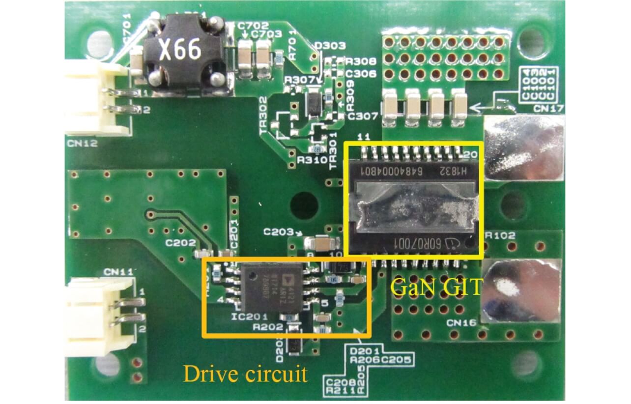
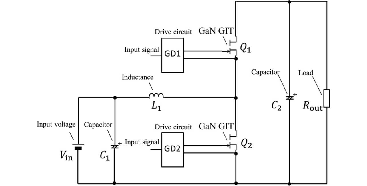
Figs. 8 and 9 show the block diagram of the evaluation board used and the synchronous rectification type DC/DC converter. The conventional circuit and the proposed circuit were applied to the gate drive circuit (GD1 and GD2), and IGOT60R070D1 (Infineon)13) was used as GaN GIT. Considering the rated operation region of the device, the evaluation was performed in the condition of the voltage boost operation of Vin = 150 V, Vout = 300 V, Pout = 0.25−1 kW, and fSW = 20 kHz. Table 2 shows the parameters used. The capacitance CP was adjusted at approximately VN =-5.0 V in order to prevent incorrect turn-on of GaN GIT caused by the miller current.
| Components | Constant | |
|---|---|---|
| Conventional circuit | Proposed circuit | |
| Rp | 330 Ω | 130 Ω |
| Rs | ― | 200 Ω |
| Rgon | 22 Ω | 22 Ω |
| Rgoff | 0 Ω | 0 Ω |
| Cp | 3.2 nF | 1.0 nF |
| Cs | ― | 22 nF |
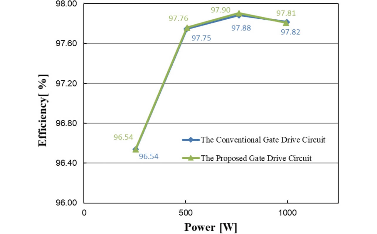
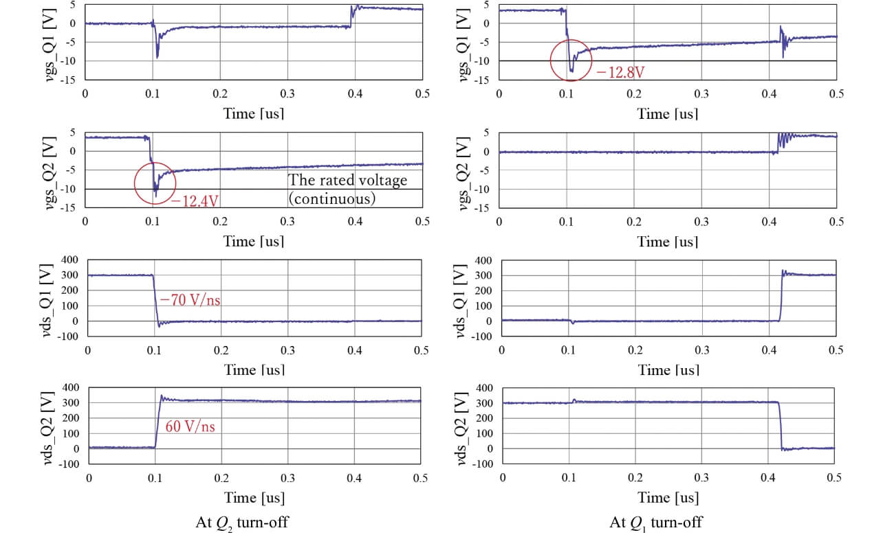
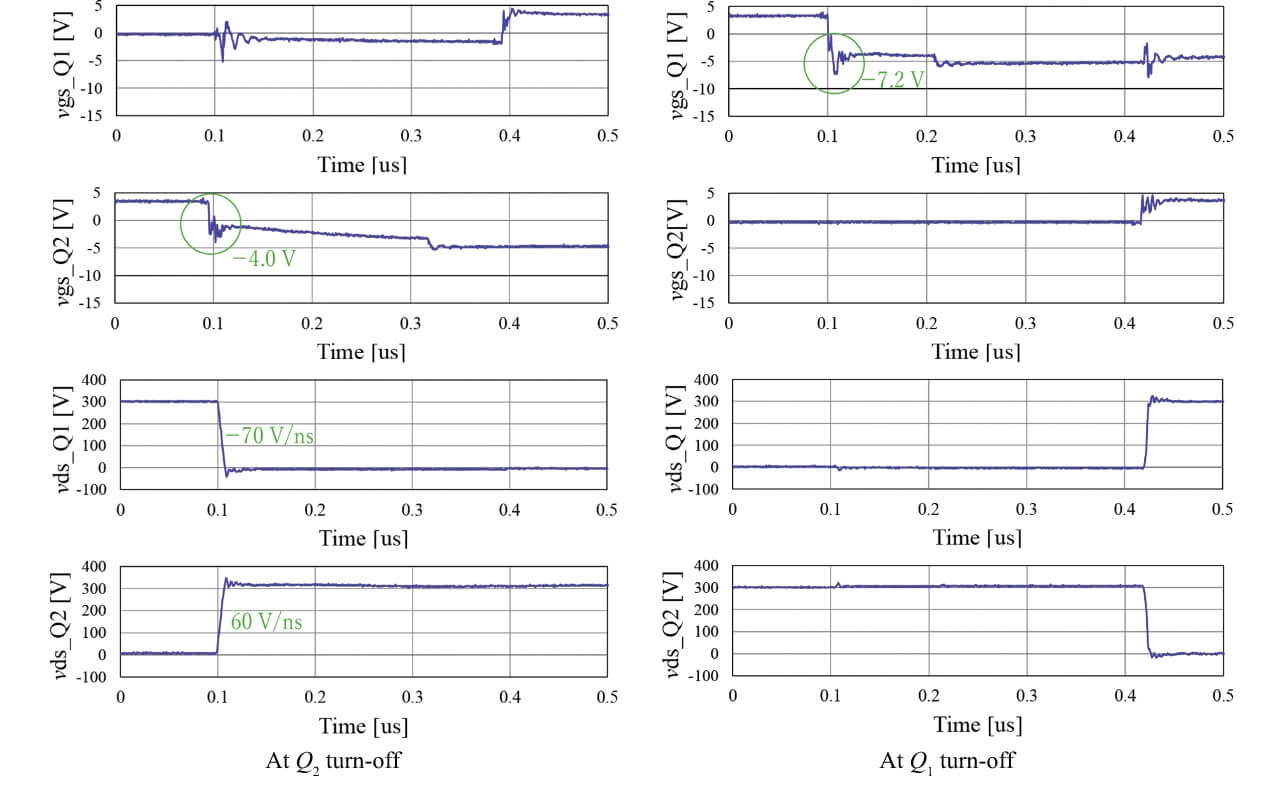
Fig. 10 shows the result of the efficiency measurement. It is found that there is no difference in efficiency between the conventional circuit and the proposed circuit. Fig. 11 shows the waveform of the conventional gate drive circuit (Fig. 11 (a)) and the waveform of the proposed gate drive circuit (Fig. 11 (b)) in the condition of Pout = 1 kW. The left and right sides show the waveforms of turn-off of the devices Q2 and Q1, respectively. The voltage signals vgs and vds were detected by the optical isolation differential probe (TIVM1 and TIVH08: manufactured by Tektronix Co.). The spike gate voltage at the turn-off of the device Q1 is -12.8 V in the conventional circuit and −7.2 V in the proposed circuit. The spike gate voltage of the proposed circuit was improved by 5.6 V in comparison with the conventional one. Similarly, the spike gate voltage of the device Q2 at the turn-off is -12.4 V in the conventional circuit and -4.0 V in the proposed circuit. The spike gate voltage of the proposed circuit was improved by 8.4 V in comparison with the conventional one. Since the proposed drive circuit can realize two-step turn-off switching at the turn-off of both devices Q1 and Q2, the generation of spike gate voltage is suppressed. Therefore, a sufficient margin can be secured for the rated gate-to-source voltage of -10 V. In addition, the switching speed of the drain-to-source voltage at the turn-off of Q1 and Q2 is not very different in comparison with the conventional circuit. Furthermore, in the proposed circuit, the miller noise that is superimposed onto the gate voltage during the switching period can be reduced, and it is considered that the low impedance of the gate circuit can be realized by the miller clamp MOSFET QS during the switching period. From these results, we were able to experimentally verify that the application of the two-step turn-off circuit allows the simultaneous satisfaction of the contrary performance of the low spike gate voltage and high speed turn-off switching.
5. Conclusions
The conventional gate drive circuit had the task that the high spike gate voltage generated at switching hinders high speed switching and higher efficiency. Therefore, this paper proposed the two-step turn-off method for the GaN GIT gate drive capable of simultaneously realizing the contrary performance of low noise and high speed turn-off switching. We mounted it to the synchronous rectification type DC/DC converter using the proposed gate drive circuit to evaluate the actual machine. We verified that the spike gate voltage was reduced by a maximum of 8.4 V without impairing the high speed turn-off switching characteristics and efficiency and showed the effectiveness of this system by securing the sufficient margin for the rated gate-to-source voltage of -10 V.
Hereafter we will study the optimization of the circuit constant matching the drive conditions.
References
- 1)
- E. A. Jones, F. F. Wang, and D. Costinett, “Review of Commercial GaN Power Devices and GaN-Based Converter Design Challenges,” IEEE J. Emerg. Sel. Top. Power Electron., vol. 4, no. 3, pp. 707-719, Sep. 2016.
- 2)
- T. Oka, T. Ina, Y. Ueno, and J. Nishii, “Over 10 A Operation with Switching Characteristics of 1.2 kV-Class Vertical GaN Trench MOSFETs on a Bulk GaN Substrate,” in Proc. 28th Int. Symp. Power Semiconductor Devices and ICs, Jul. 2016, pp. 459-462.
- 3)
- O. Hilt, E. Treidel, M. Wolf, C. Kuring, K. Tetzner, H. Yazdani, A. Wentzel, and J. Würfl, “Lateral and Vertical Power Transistors in GaN and Ga2O3,” IET Power Electron., vol. 12 no 15, pp. 3919-3927, Dec. 2019.
- 4)
- H. Hahn et al., “p-Channel Enhancement and Depletion Mode GaN-Based HFETs With Quaternary Backbarriers.” IEEE Transactions on Electron Devices, vol. 60, no. 10, pp. 3005-3011, Oct. 2013.
- 5)
- Y. Cai, Y. Zhou, K. Chen, and K. Lau, “High-Performance Enhancement-Mode AlGaN/GaN HEMTs Using Fluoride-Based Plasma Treatment.” IEEE Electron Device Lett., vol. 26, no. 7, pp. 435-437, Jul. 2005.
- 6)
- X. Huang, Z. Liu, Q. Li and F. C. Lee, “Evaluation and Application of 600 V GaN HEMT in Cascode Structure.” IEEE Transactions Power Electon., vol. 29, no. 5, pp. 2453-2461, May 2014.
- 7)
- Y. Uemoto et al., “Gate Injection Transistor (GIT)- A Normally-Off AlGaN/GaN Power Transistor Using Conductivity Modulation,” IEEE Trans. Electron Devices, vol. 54, no. 12, pp. 3393-3399, Nov. 2007.
- 8)
- T. Morita, H. Handa, S. Ujita, M. Ishida, and T. Ueda, “99.3% Efficiency of Boost-Up Converter for Totem-Pole Bridgeless PFC Using GaN Gate Injection Transistor,” in Proc. Int. Exhib. Conf. Power Electron., Intell. Motion, Renewable Energy and Energy Manag., PCIM Europe., May 2014, pp. 325-329.
- 9)
- H. Li, C. Han, J. Brothers, X. Zhang, and J. Wang, “Evaluation of 600 V GaN based gate injection transistors for high temperature and high efficiency applications,” 2015 IEEE 3rd Workshop on Wide Bandgap Power Devices and Applications (WiPDA), Nov. 2015, pp. 85-91.
- 10)
- Y. Abdullah, H. Li, and J. Wang, “Evaluation of 600 V Direct-Drive GaN HEMT and a Comparison to GaN GIT,” IEEE 5th Workshop on Wide Bandgap Power Devices and Applications (WiPDA), Nov. 2017, pp. 273-276.
- 11)
- D. Bortis, O. Knecht, D. Neumayr, and J. W. Kolar, “Comprehensive Evaluation of GaN GIT in Low- and High-Frequency Bridge Leg Applications,” in 2016 IEEE 8th Int. Power Electron. Motion Control Conf. (IPEMC-ECCE Asia), May 2016, pp. 21-30.
- 12)
- B. Zojer, 600 V CoolGaN™ high electron mobility transistors. AN_201702_PL52_012, Infineon Technologies AG, 2018.
- 13)
- Infineon Technologies AG, “IGOT60R070D1, 600V CoolGaN™ enhancement-mode power transistor,” datasheet, 2020.
The names of products in the text may be trademarks of each company.