


Noise Cancellation for Miniaturization of Switched Mode Power Supply
- Switched Mode Power Supply
- Noise Cancelling
- Miniaturization
- Power factor correction
In recent years, it has been necessary to improve operational efficiency and reduce costs by using AI and IoT in the manufacturing industry to reduce the impacts from the shortage of skilled workers and increased labor costs. To meet these requirements, the amount of equipment in the control panel is increasing, and the space for new equipment is an important issue. The power supply occupies a large space in the control panel and must be reduced in size. In general, miniaturization of power supplies has been realized by higher switching frequencies. However, higher switching frequencies increase noise emission levels and require an additional EMI filter. We propose a new noise cancellation design process that optimizes the tradeoff between current injection capacitance and auxiliary winding voltage by adjusting the turn ratio of the cancellation winding. By applying this design process to a 100 to 240 V AC, 480 W output power supply, the volume of the EMI filter is reduced by approximately 50%, and the overall power supply volume is reduced by approximately 10%.
1. Introduction
1.1 Significance of the miniaturization of switched-mode power supplies
In recent years, the manufacturing industry is finding it necessary to promote AI- or IoT-driven work efficiency improvement and cost reduction to alleviate the negative impacts from the labor shortage and soaring labor costs due to the shrinking population. To meet such needs, OMRON develops a wide range of equipment that delivers functions of equipment diagnosis and life expectancy prediction. For use on a manufacturing site, these pieces of equipment must be installed in the production line control panel at the factory. Existing control panels have limited space to accommodate the installation of new equipment. At the same time, there are also demands for space-saving control panels. What is necessary to meet these conflicting needs is to miniaturize switched-mode power supplies that occupy particularly large spaces inside control panels.
1.2 Challenges to the miniaturization of switched-mode power supplies
Fig. 1 shows a typical configuration of a several hundred-Watt-class switched-mode power supply for use in control panels. The switched-mode power supply connects directly to the commercial AC mains and therefore consists mainly of the following three circuits: an input EMI filter, a power factor correction (PFC) circuit, and an isolated DC-DC circuit1).
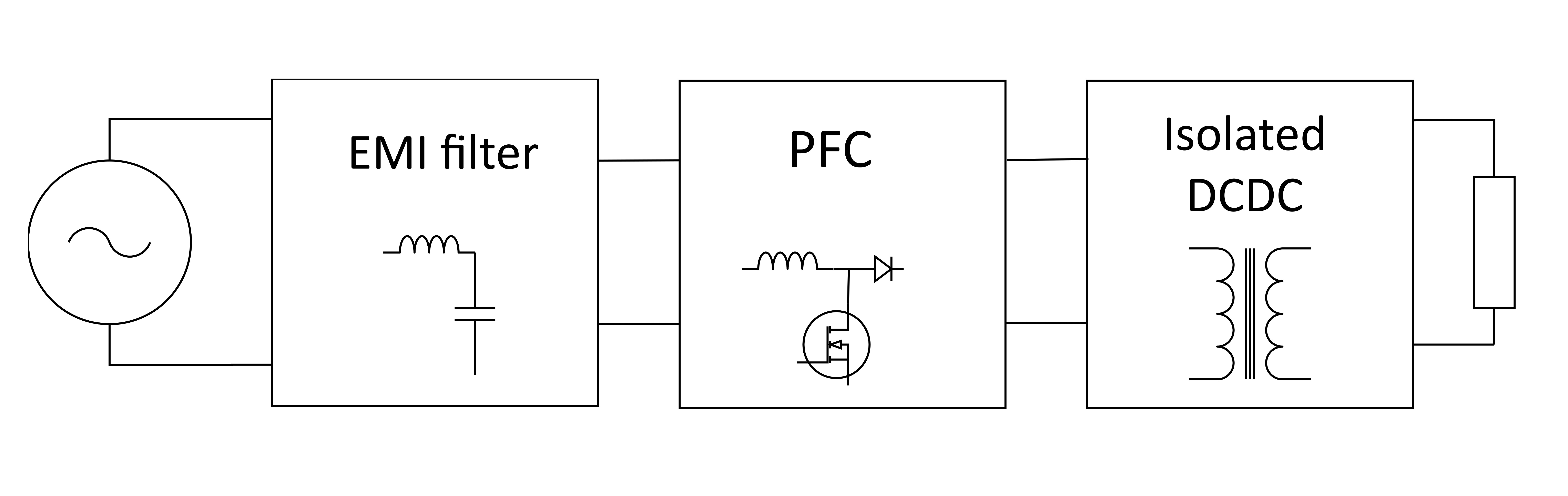
In a typical configuration, these circuits account for approximately 20%, 35%, and 35% of the overall volume, respectively. While methods of miniaturization have been studied for the respective circuits, this paper limits its scope to describing the miniaturization of the EMI filter. Note, however, that in light of the close relationship between the noise-source PFC circuit and the EMI filter, this paper provides descriptive coverage ranging from the mechanism of the noise generation in the PFC circuit to the noise reduction measures for the EMI filter.
PFC circuit miniaturization has been achieved by taking full advantage of low-loss power semiconductors made available by passive parts (magnetic parts and capacitors) miniaturized through frequency enhancement. As a side effect of frequency enhancement, noise components have come to have higher frequencies, giving rise to the problem of larger EMI filter sizes2).
1.3 Our proposed noise cancellation method
The methods generally employed for noise reduction are filtering and canceling methods. Because its purpose is to reduce high-frequency noise, this study made inquiries with the focus on a noise cancellation method. Among the noise cancellation methods explored in previous studies is one that adds a noise cancellation winding to a PFC voltage boost inductor3). On the one hand, this method uses a primary winding and an auxiliary winding at the same turn ratio (1:1) and hence is ideal from the viewpoint of the noise cancellation effect. On the other hand, however, such a method has the drawback of causing high voltage, thereby necessitating increases in the circuit board size because of the relevant safety constraints (e.g., creepage distance). Another previous study proposed as a solution a method that sets the turn ratio on the noise cancellation winding for a PFC voltage boost inductor to  :14). The study, however, failed to say anything about the optimization of the and the capacitance.
We propose to adjust the turn ratio of :1 on the noise cancellation winding for a PFC voltage boost inductor to optimize the tradeoff between the noise cancellation winding voltage and the noise cancellation current injection capacitance. This optimization is intended to strike an optimal balance between the noise reduction effect and EMI filter miniaturization.
Chapter 2 explains the mechanism of the noise generation in the PFC circuit, while Chapter 3 describes our proposed noise cancellation method based on the existing winding of the PFC circuit. Chapter 4 explains the optimization of the relevant parameters, while Chapter 5 demonstrates by simulation and experiment the effectiveness of our proposed method. Chapter 6 presents the results of an actual EMI measurement test. Chapter 7 presents a summary of this paper and a description of the effect of miniaturization in products.
2. Mechanism of noise generation in the PFC circuit
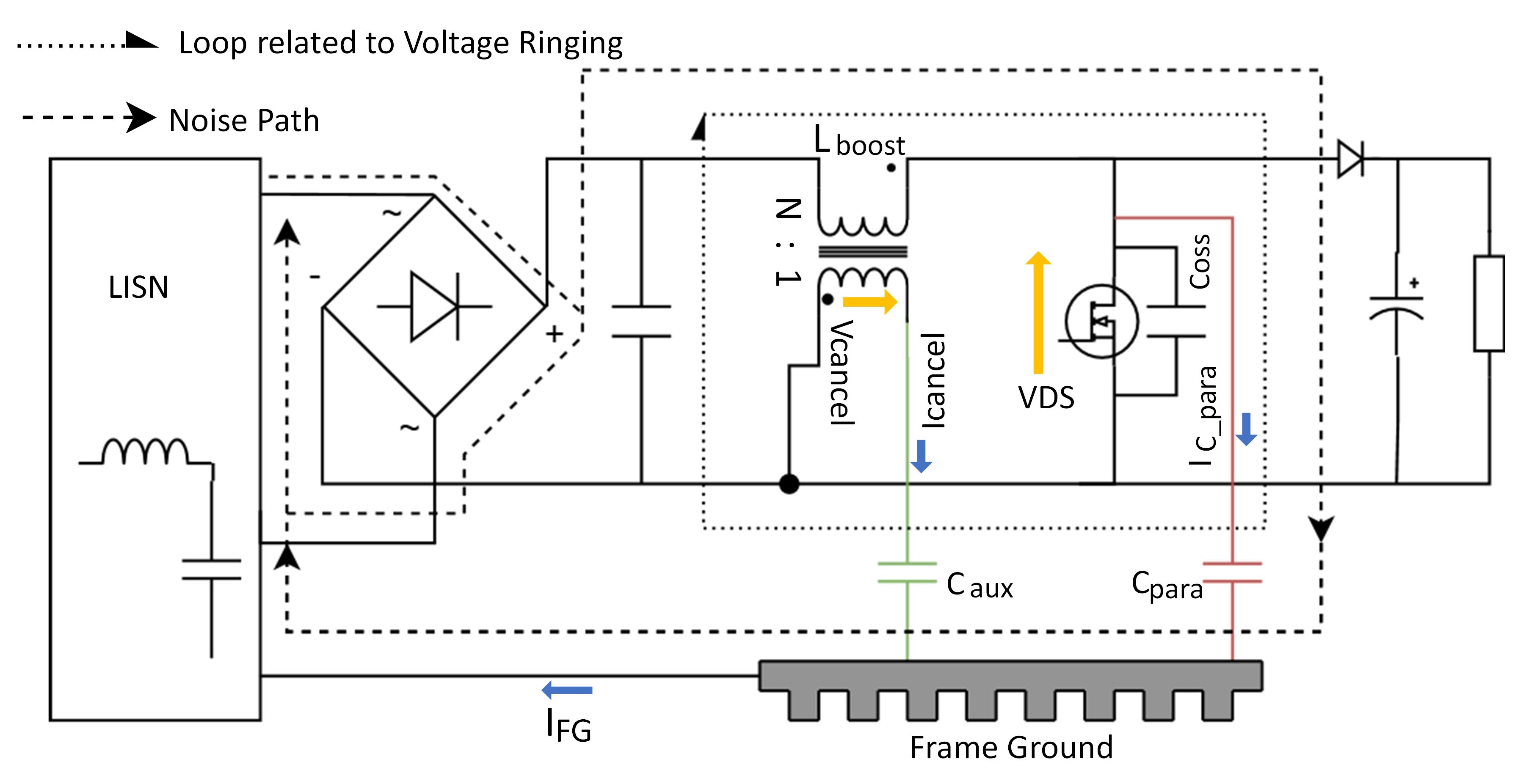
The main noise generated in a switched-mode power supply circuit is common-mode noise. The causes of PFC common-mode noise include (1) the mode conversion of differential-mode currents and (2) currents that occur because of voltage fluctuations in the power semiconductor and contribute to the frame ground (FG) potential5)-6). The latter, in particular, is described in more detail because it dominates the noise emission level.
Fig. 2 shows a typical block diagram of a PFC circuit, while Fig. 3 shows a typical behavior of inductor current during the half cycle of the commercial AC mains (50 Hz or 60 Hz). Generally, a continuous current mode (CCM) PFC control circuit operates in CCM mode during the rated load operation mode and switches to the discontinuous current mode (DCM) under a light load. The noise generated during this DCM mode operation was the cause of the increases in EMI filter size. The reason is presented below.
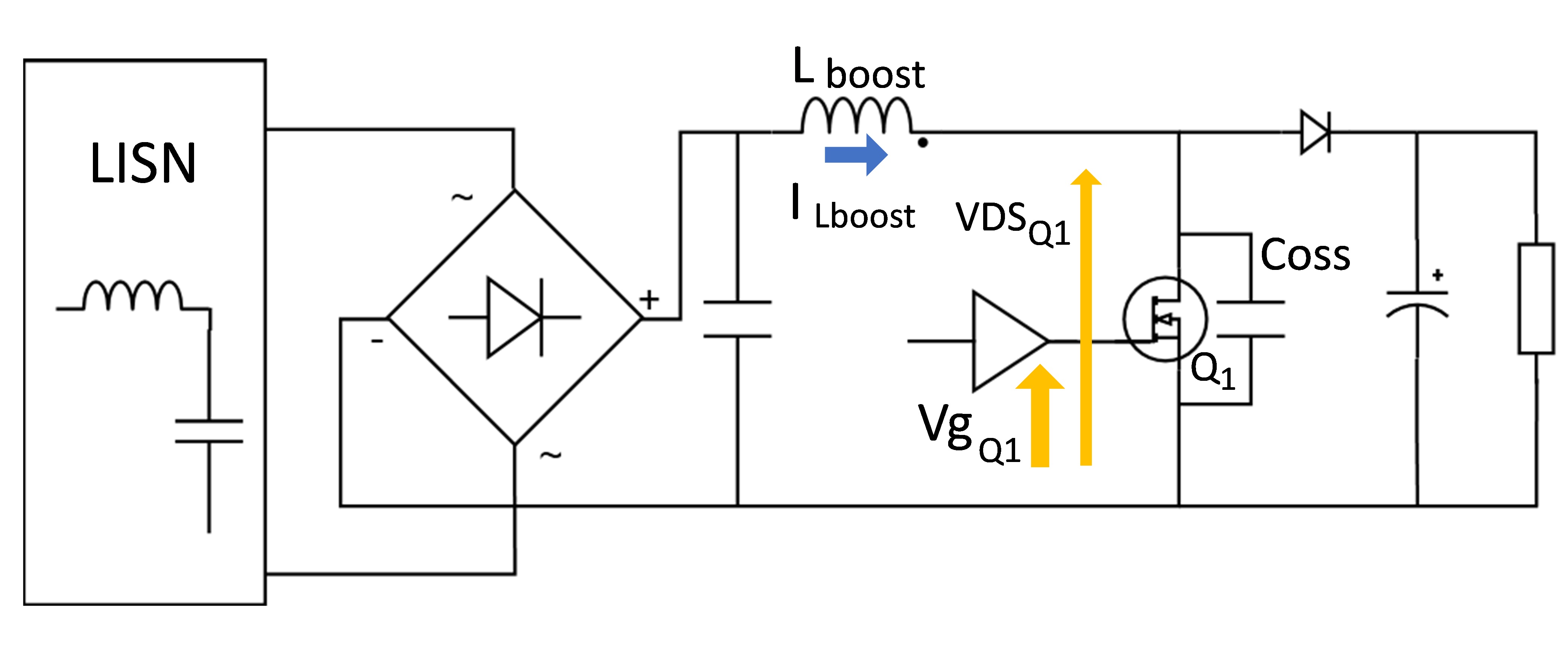
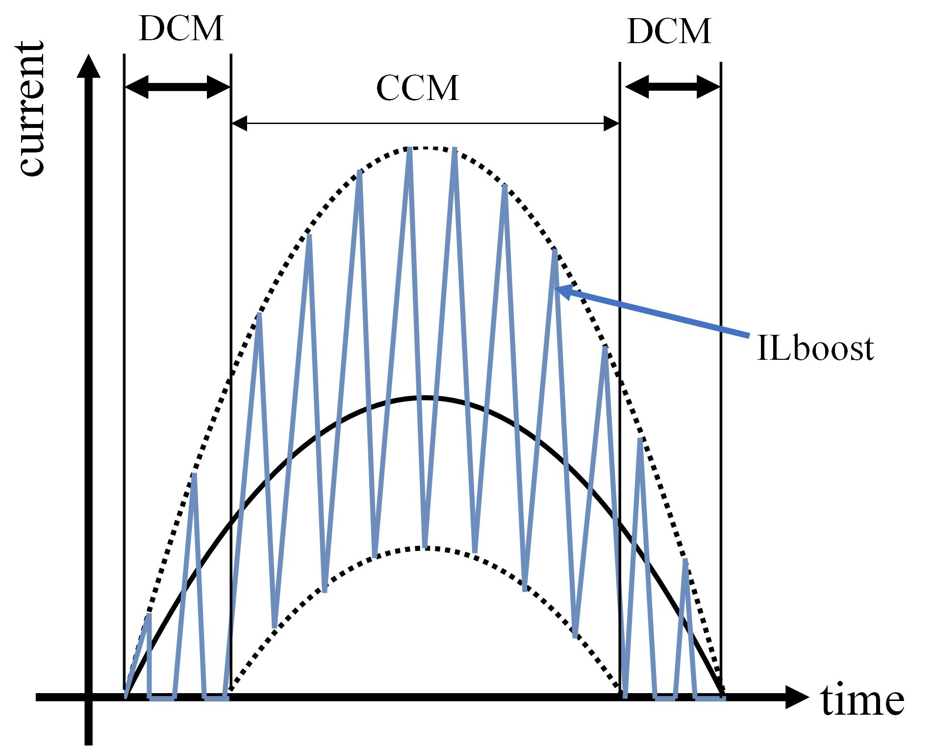
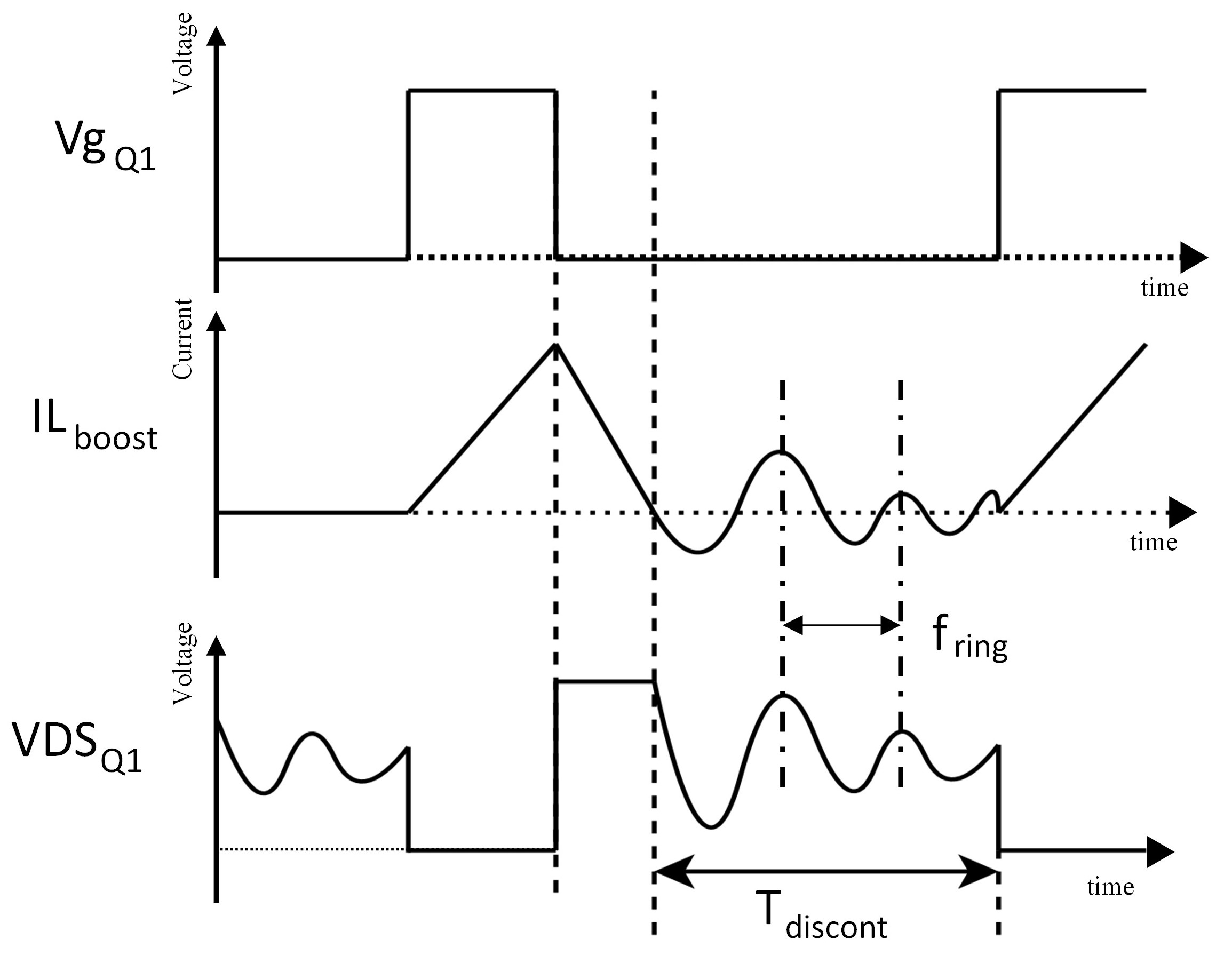
Fig. 4 shows typical switching waveforms during DCM operation. During the non-conduction period  of DCM operation, a resonance circuit is formed between the power semiconductor Q1 output capacitance
  and the voltage-boost inductance
  , thereby causing free oscillations observable as voltage ringing between the drain and source of the power semiconductor. The voltage ringing frequency observed here is expressed by Equation (1):

A conversion of the PFC switching frequency into a high frequency would result in a decrease in the inductance value , but the output capacitance would remain the same. Hence, it follows from Equation (1) that the voltage ringing frequency would increase. The observable noise would increase on the high-frequency side because of the decrease in the noise reduction effect of the EMI filter.
Let us explain here the mechanism in which this voltage ringing propagates in the form of a noise current via the parasitic capacitance of the power semiconductor and undergoes conversion into a common-mode noise.
As shown in Fig. 5, the power semiconductor is connected to the FG-potential heat sink for heat radiation. The electric potential fluctuations in the drain terminal, which serves as the cooling surface for the power semiconductor, cause a coupling capacitance  between the semiconductor and the heat sink, thereby resulting in a current
  that contributes to the FG potential. This current flows as a common mode current
  to the FG. Fig. 6(a) shows the and waveforms for the case without noise cancellation current. This flows into the outside of the switched-mode power supply circuit in such a manner as to appear as a common-mode noise as seen from equipment other than the switched-mode power supply.
 :1
:1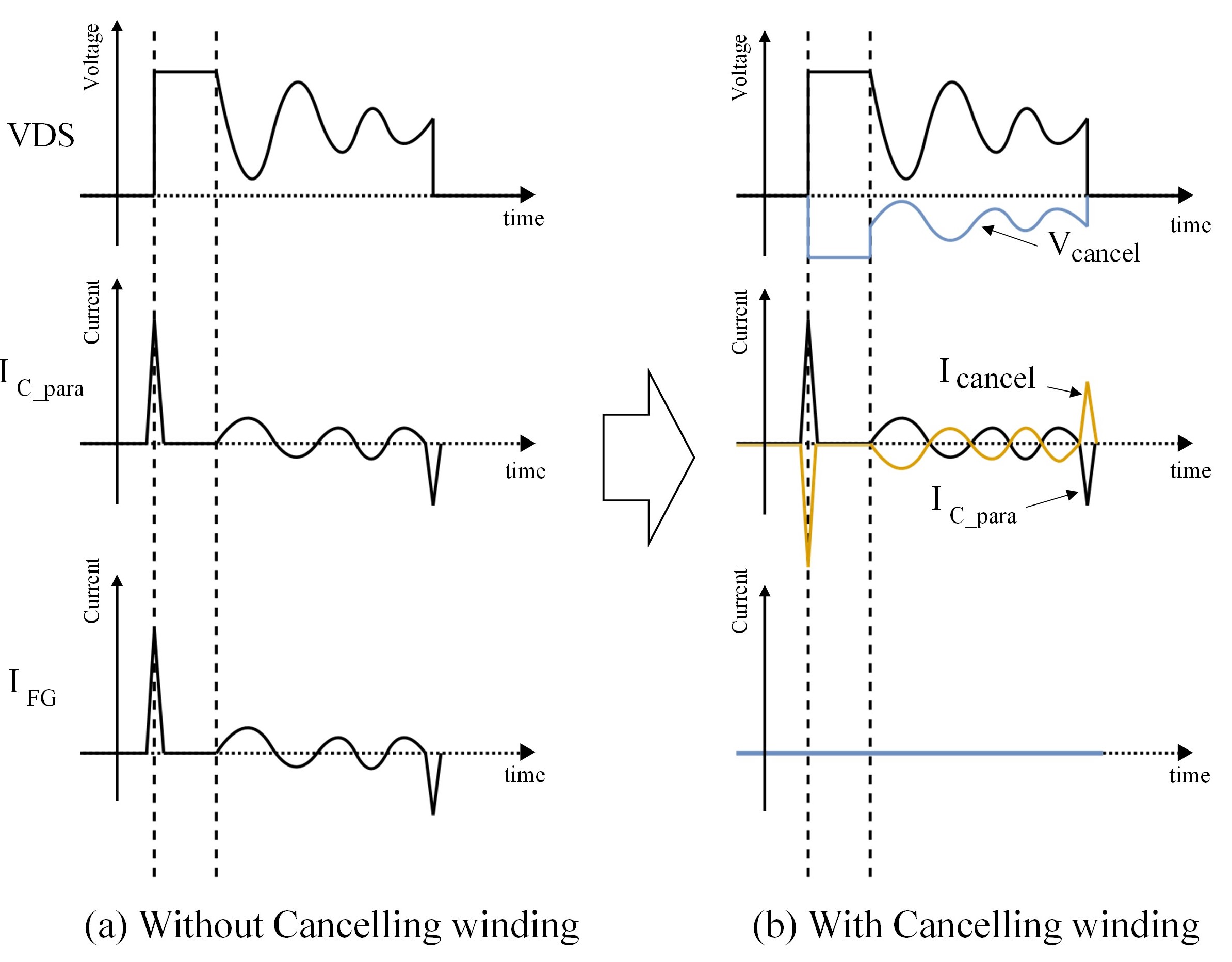
The voltage ringing expressed by Equation (1) causes an increase in the electric potential fluctuations in the drain terminal of the power semiconductor. Hence, as shown in Fig. 6(a), increases, thereby resulting in an increase in common-mode noise.
3. Our proposed noise cancellation method
With the noise cancellation method applied, the current  with its phase reverse to that of flows into the FG potential, so that and cancel each other to reduce and hence the common-mode noise as shown in Fig. 6(b). This study added some ingenuity to the following two points to provide a noise cancellation winding on a voltage boost inductor: (1) adjusting the turn ratio on the auxiliary winding for the voltage boost inductor to :1 to reduce the auxiliary winding voltage, and (2) optimizing the balance between this turn ratio and the noise cancellation current injection capacitance to produce a noise reduction effect sufficient to achieve EMI filter miniaturization.
The addition of a noise cancellation winding with a turn ratio of :1 to the voltage boost inductor in Fig. 5 leads to the generation of the voltage  with its phase reverse to that of the VDS as Fig. 6(b) shows. The peak value
  is expressed by Equation (2):

where the  peak value is equivalent to the PFC output voltage
  , and hence can be expressed using . Equation (2) shows that is adjustable by . An increase in and the reduction in to a voltage equivalent to that of an existing auxiliary power supply winding allow a relaxation of the requirements for the creepage distance to other patterns.
Meanwhile, for complete noise current cancellation, a current with its phase reverse to that of and its equivalent magnitude is necessary as Fig. 6(b) shows. Because the current flowing to the capacitor is proportional to the differential of the applied voltage, and are expressed by the following equations, respectively:


where  is the voltage applied to the capacitor for noise cancellation current injection,
  is the voltage applied to , and the peak value of is equivalent to the VDS peak value. It follows from Equations (3) and (4) and
  that is expressed by Equation (5) when it satisfies
  :
:

The above observation reveals that is adjustable by . A smaller allows a decrease in noise cancellation current injection capacitance, thereby enabling the miniaturization of the circuit per se.
4. Parameter optimization
Chapter 3 showed that improves with a larger (small type), whereas improves with a smaller (small type). Therefore, is optimized under the conditions in Table 1:
| MOSFET-to-FG parasitic capacitance | 33 pF |
|---|---|
| Voltage boost inductor | 98 μH |
| Number of turns on the primary side of the Voltage boost inductor |
36.5 Ts |
| Output voltage Vout | 383 V |
| Maximum capacitance Caux | 1,000 pF |
| Maximum voltage Vcancel_peak | 40 V |
| Type of Caux | Murata Manufacturing Co., Ltd., DE1 KX Series |
Considering the size of the part, the maximum capacitance in Table 1 was specified as 1,000 pF, which is the maximum capacitance available in the lineup of capacitors with an outside diameter of 8 mm. Meanwhile, the maximum voltage was set to 40 V max., considering the applicable safety standards. Fig. 7 shows the plots of Equation (2) and Equation (5) based on Table 1:
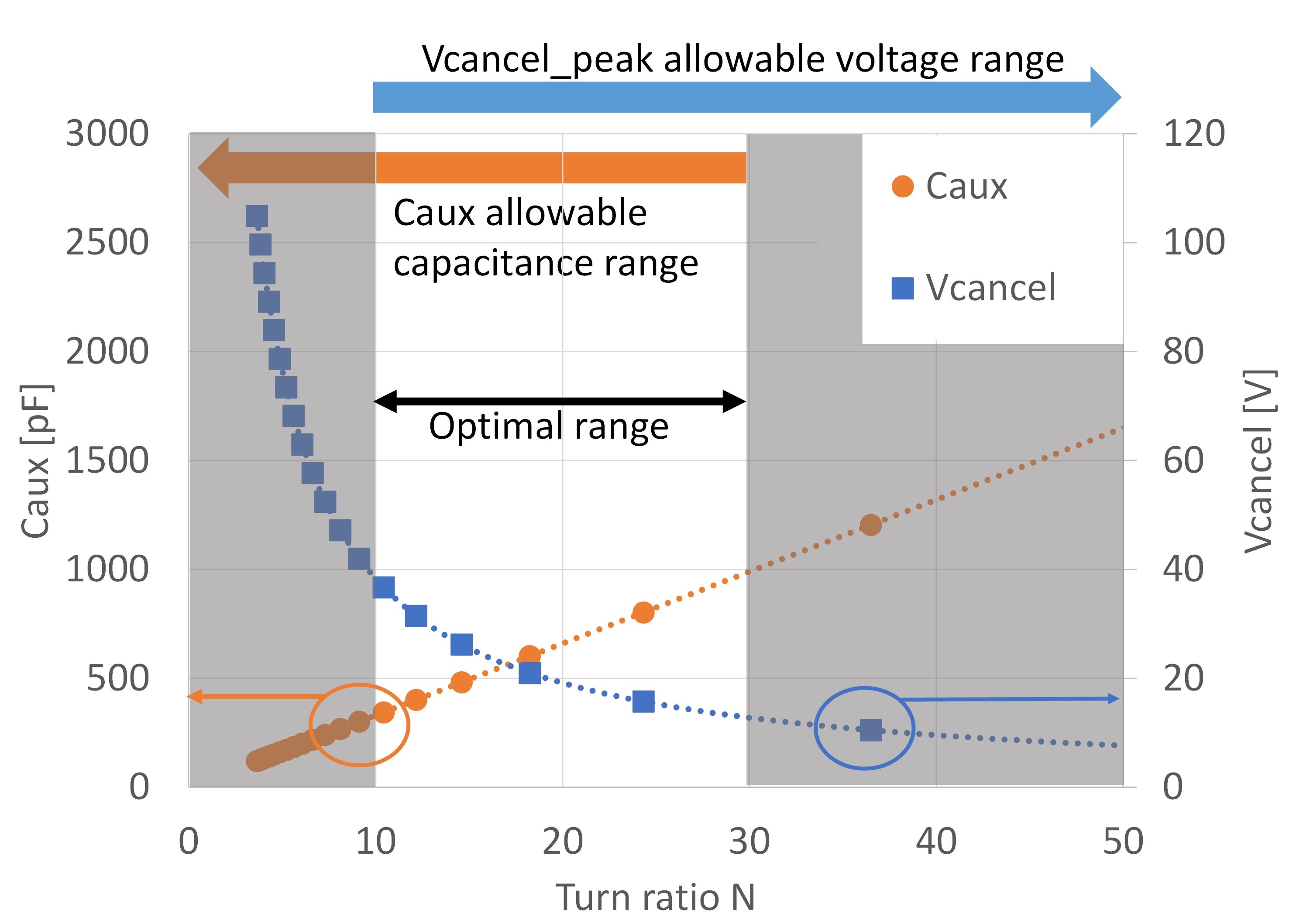 and capacitance relative to the change in the number of turns on the auxiliary winding
Considering the maximum voltage , the turn ratio should be 10 or more. Additionally, considering the maximum capacitance , the turn ratio should be less than 30. Thus, the available range for the turn ratio is from 10 or more to less than 30. The turn ratio selected this time is 18.25, which falls near the center of the available range (the number of turns on the auxiliary winding = 2 Ts). Here, the voltage is approximately 21 V. From Equation (5), the capacitance is determined as approximately 600 pF. This value is, however, the one to be selected for complete noise current cancellation. This paper aimed at achieving a halved noise current as a noise cancellation effect because the results of a preparatory noise measurement had shown that it would suffice to reduce the noise level by approximately 6 dBμV. Hence, the capacitance was set to 330 pF, an approximately half of 600 pF. Fig. 8 shows the operation waveforms with set to 330 pF:
 set to 330 pF
5. Simulation and experimental results
To examine the resonant operation waveforms generated as a result of our proposed noise cancellation method, a simulation and an experimental observation on an actual unit were performed based on the parameter optimization results. Table 2 shows the simulation parameters and the specifications for the power supply used for the experiment:
| Input voltage | 100-240 V AC, 240 V AC during test |
|---|---|
| output voltage | 24 V |
| rated output power | 480 W |
| PFC switching frequency | 140 kHz |
| MOSFET Co(er) | 123 pF(VDS = 0-400 V, Vgs = 0 V) |
| Voltage boost inductor (inductance, turn ratio) | 98 μH: 36.5, Ts = 2 Ts |
| Caux | 330 pF |
Fig. 9 shows the simulation waveforms. It was found that the voltage ringing during DCM operation caused the noise current and that the noise cancellation current was a current with its phase reverse to that of with its magnitude approximately half. It was confirmed that the noise current was reduced to approximately 1/2 of as expected. Moreover, with the number of turns on the auxiliary winding set to 2 Ts for the primary winding with 36.5 Ts per phase, the voltage was successfully reduced to 40 V or less. Note that the voltage ringing frequency in this simulation was 565 kHz.
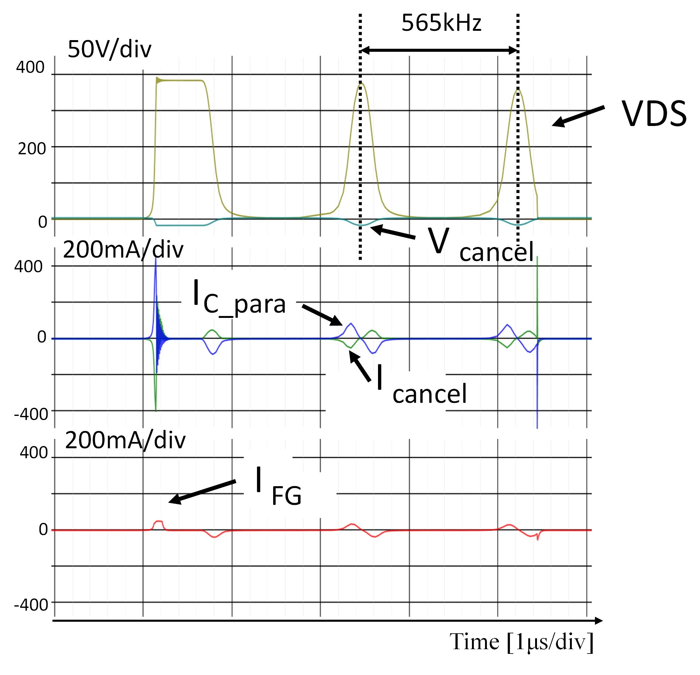
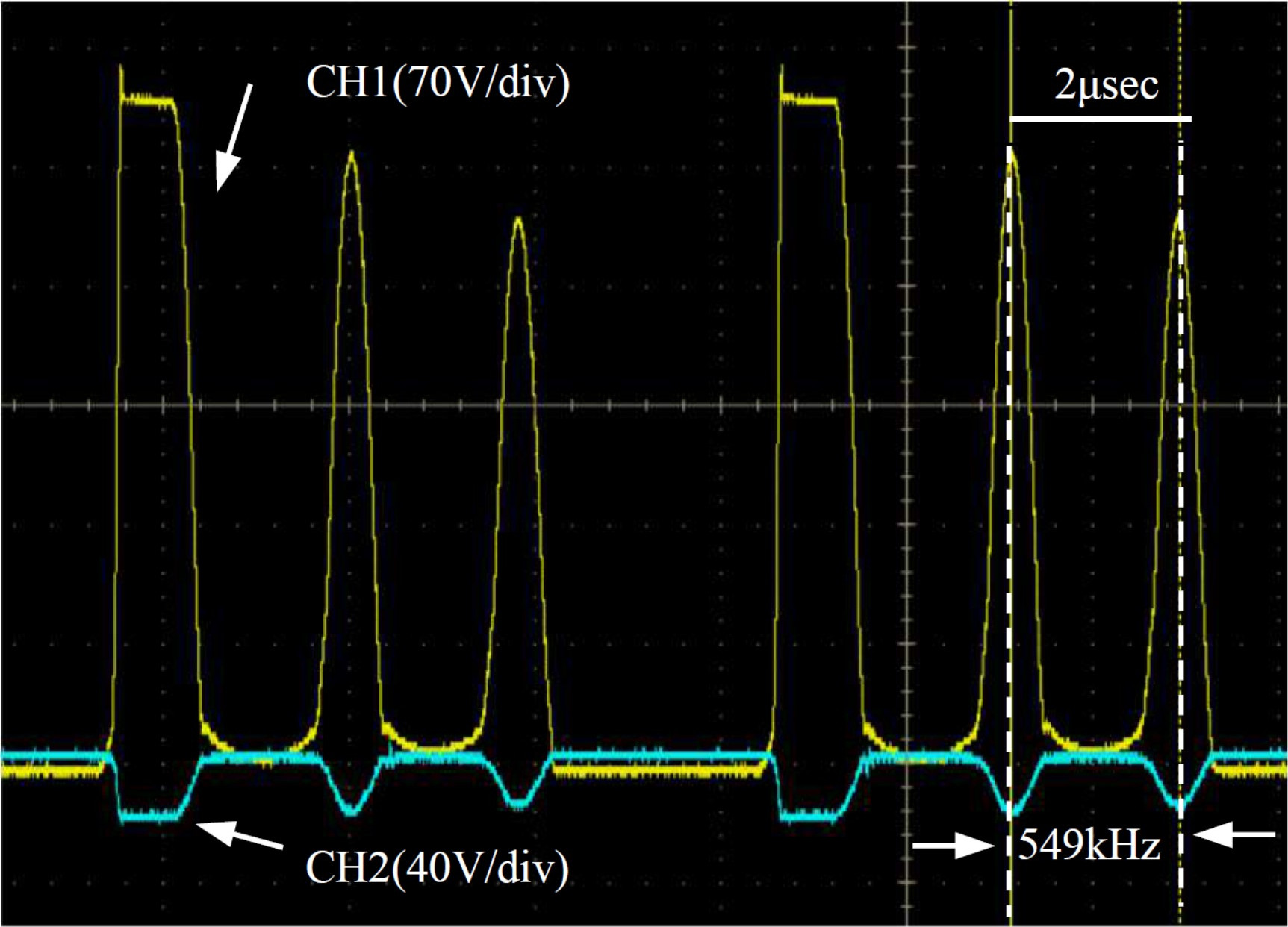
Fig. 10 shows the actual waveforms observed in the actual unit. The voltage ringing during DCM operation and the reverse-phase voltage induced by the auxiliary winding were observed. The voltage ringing frequency observed then was 549 kHz. The ringing frequency is difficult to determine by calculation because of the voltage dependence of the output capacitance Coss of the power semiconductor. Therefore, Fig. 9 simulation results reflecting the voltage dependency of are considered valid.
6. Conductive noise measurement results
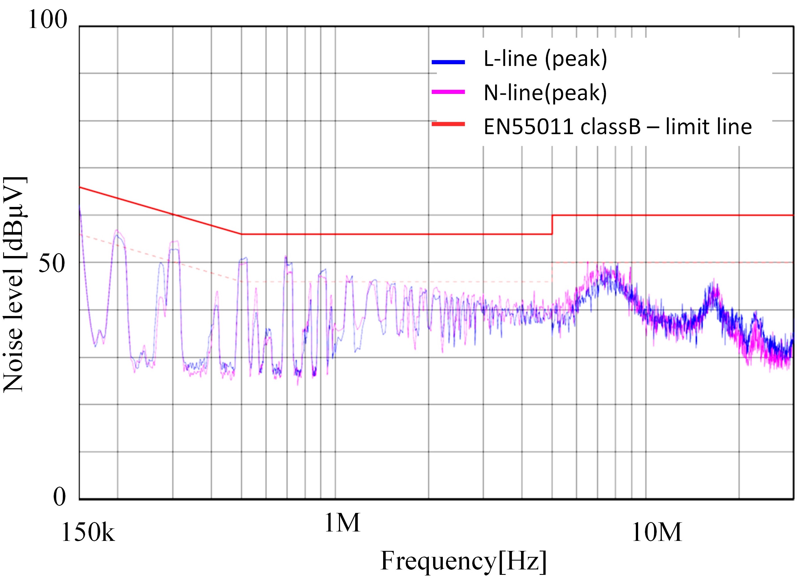
To verify the effectiveness of our proposed noise cancellation system, a conventional dual-stage EMI filter was miniaturized into a single-stage configuration and set on an actual unit to undergo conductive noise measurement. Fig. 11 shows the results of conductive noise measurement without noise cancellation, while Fig. 12 shows the results of that performed with our proposed noise cancellation. The measurements shown in both Figs. 11 and 12 were taken as per EN 55011 Class B, a noise-related standard. The vertical and horizontal axes in each figure represent the noise level and the frequency, respectively.
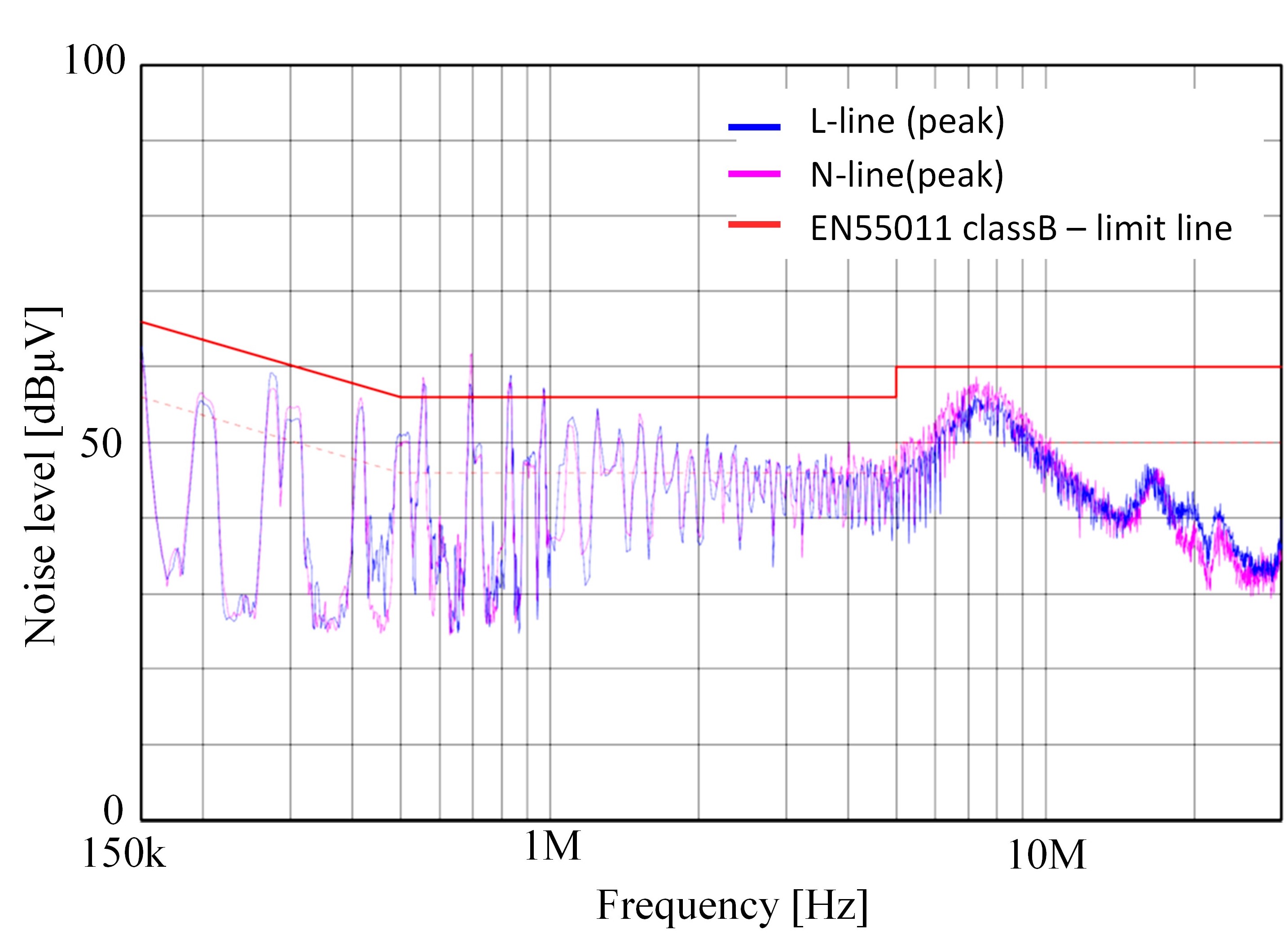
In Fig. 11, the noise levels at the harmonics (280 kHz, 420 kHz, …) of 140 kHz, the PFC switching frequency, remained relatively high throughout the observation. Also observed were increases in noise characteristic to the vicinity of 560 kHz, 700 kHz, 840 kHz, and 980 kHz, in other words, the fourth- to seventh-order harmonics of 140 kHz. Considering that the ringing frequency of the VDS voltage is 549 kHz in Fig. 10, the noise near 560 kHz in Fig. 11 probably resulted from the superimposition of the voltage ringing. Similarly, the VDS voltage ringing at 700 kHz, 840 kHz, and 950 kHz was observed with the actual unit, suggesting that the cause was the ringing frequency superimposed on the harmonics of the PFC switching frequency. It turned out that without our proposed noise cancellation method, the EMI filter failed the noise test because of some frequency bands in which noise peaks exceeded the limit value specified in EN 55011 Class B.
Fig. 12 reveals that our proposed noise cancellation method helped to reduce the noise peaks of the harmonics of the PFC switching frequency and those of the VDS voltage ringing frequency by 5 to 10 dB. Thus, the test results show that even with a single-stage EMI filter, the noise peaks at all frequencies sufficiently meet EN 55011 Class B. The above results confirm the effectiveness of our proposed noise cancellation system.
7. Conclusions
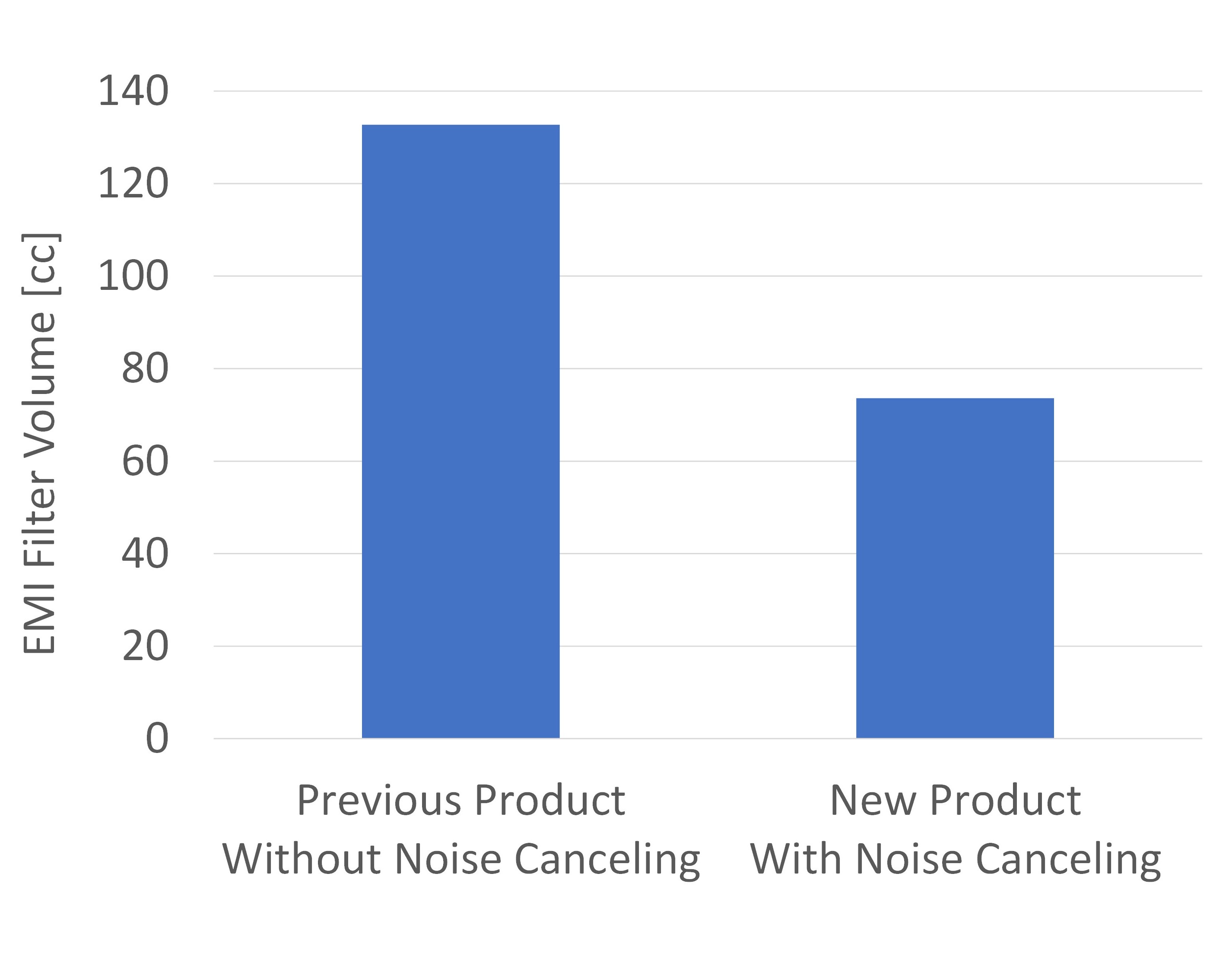
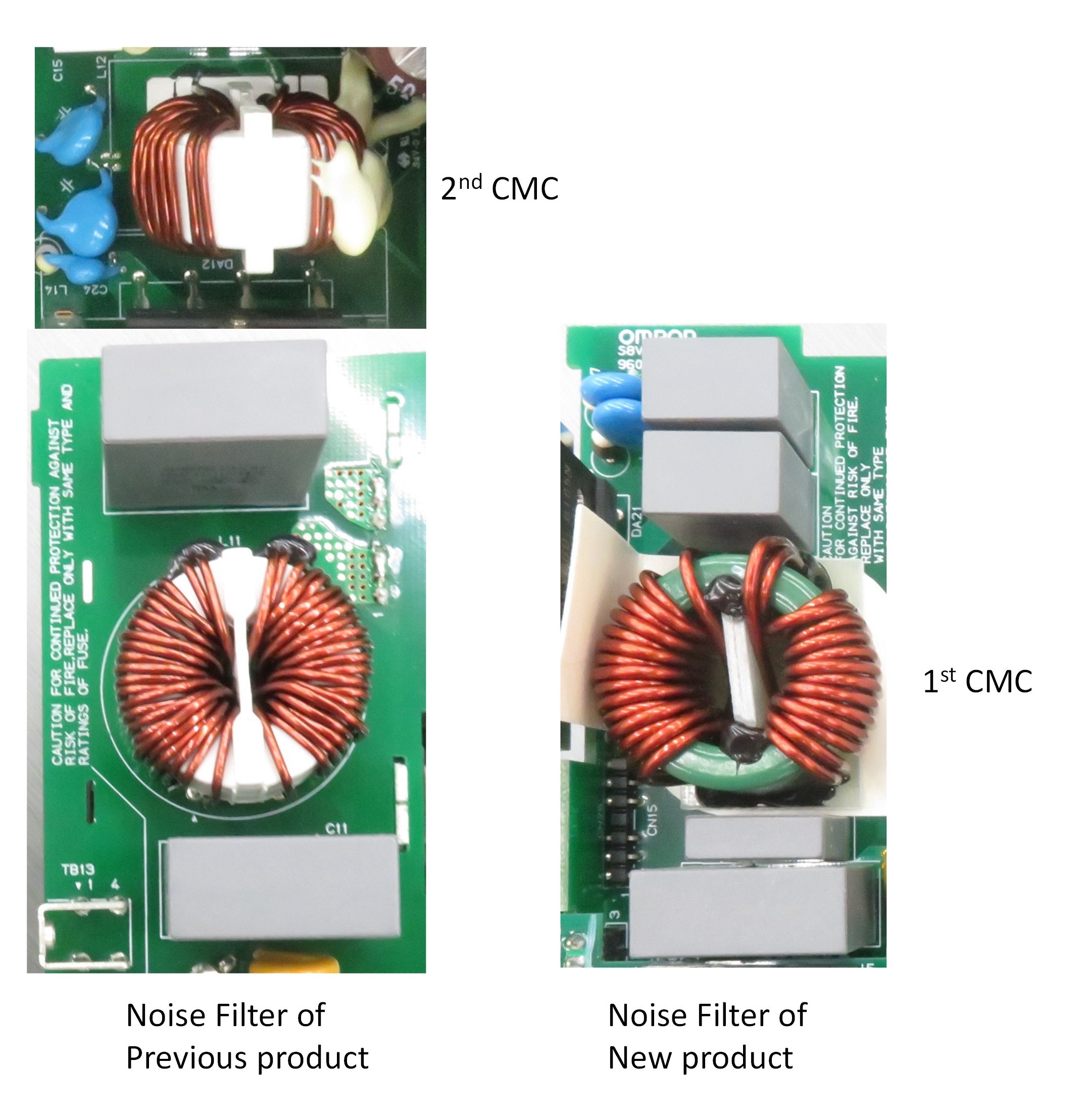
This paper proposed a new design method that allows noise cancellation as a solution to the problem of EMI filter size increases that result from the increase in harmonic common-mode noise induced by the switching frequency as a result of frequency enhancement. This method adjusts the turn ratio of :1 on the noise cancellation winding added to the PFC voltage boost inductor to optimize the noise cancellation winding voltage and the noise cancellation current injection capacitance thereby achieving noise reduction and EMI filter miniaturization at the same time. To demonstrate the effectiveness of our proposal, a verification test was performed by simulation using an actual unit. As a result, it was observed that even a singlestage EMI filter reduced conductive noise by approximately 10 dBμV as compared to when used without noise cancellation. Thus, it was confirmed that our proposed noise cancellation method provides a sufficient noise cancellation effect. Fig. 13 shows the miniaturization effect with our proposal applied, while the photos in Fig. 14 show the actual shapes of the conventional and new filters. Our proposed method allowed an approximately 50-percent volume reduction in EMI filter volume compared to the conventional EMI filter that accounted for approximately 20% of the overall power supply volume. The overall power supply volume was reduced by 10 percent (= 50% × 20%) as compared to that before the application of our proposed method.
References
- 1)
- Power Electronics Handbook Compilation Committee (ed.), Power Electronics Handbook (in Japanese), Ohmsha, p. 717, 2010.
- 2)
- B. Lu, W. Dong, S. Wang, and F.C. Lee, “High Frequency Investigation of Single-switch CCM Power Factor Correction Converter”, in Proc. Applied Power Electronics Conference and Exposition. 2004, Vol. 3, pp. 1482-1487.
- 3)
- D. Cochrane, D.Y. Chen, and D. Boroyevic, “Passive Cancellation of Common-Mode Noise in Power Electronic Circuits”, IEEE Transactions on Power Electronics, Vol. 18, No. 3, pp. 756-763, 2003.
- 4)
- M. Schmidt, J. Stahl, and M. Albach, “Influence of Parasitic Effects on Passive Cancellation of Common Mode Noise in a Boost Converter,” in Proc. Applied Power Electronics Conference and Exposition, 2004, pp. 471-477.
- 5)
- S. Wang and F. C. Lee, “Investigation of the Transformation Between Differential-Mode and Common-Mode Noises in an EMI Filter Due to Unbalance,” IEEE Transactions on Electromagnetic Compatibility, Vol. 52, No. 3, pp. 578-587, 2010.
- 6)
- T. Intachot, W. Klungwijit, Y. Prempraneerach, and S. Nitta, “A Study on Common-Mode Noise Generation in Switching Circuit due to Unbalanced Characteristic,” in Proc. Power Conversion Conference-Nagoya, 2007, pp. 429-434.
The names of products in the text may be trademarks of each company.