


Study and development of low-noise MEMS acoustic sensors
- MEMS acoustic sensor
- Slit diaphragm structure
- Reduction of self-noise
- Layout of narrow-pitch openings
- Etching process stabilization technology
Acoustic sensing technology like speech recognition or noise cancellation has attracted a lot of attention recently. These new applications stimulate the demand for smaller and lower noise MEMS (micro electro-mechanical system) acoustic sensors. Micro-scale sensors are susceptible to self-noise caused by air damping. Therefore, understanding and controlling air damping is crucial for designing low noise sensors.
In this paper, we report a novel design of MEMS acoustic sensors that achieves SNR (signal-to-noise ratio) over 68 dB. We simulated dominant noise sources based on equivalent circuit analysis and introduced original structures that significantly reduce squeeze air film damping. This new design has been successfully commercialized due to matured process stability techniques of thin-film. The acoustic sensors we developed can be widely used in applications that require small-scale and precise acoustic sensing.
1. Introduction
A trend toward mounting various sensors on various instruments or living organisms to collect data and use the obtained data for livelihoods and industries has been growing day by day. Under such circumstances, expectations are high for small and highprecision sensor devices. Micro electro-mechanical system (MEMS), which is a microfabrication technology to which semiconductor process technology is applied, is an effective method which enables downsizing, increased precision and reduced power consumption. Omron have practically realized pressure sensors and flow sensors based on MEMS technology.
Generally, downsizing a sensor reduces its sensitivity and makes it easier to be buried in the noise generated by the sensor itself. In the case of MEMS which is miniaturized further to micrometer scale, since it is significantly affected by thermal fluctuation, the influence of noise is a greater problem 1). Thus, design method of low-noise MEMS sensors is an important theme.
The above circumstance is the same with microphones (hereinafter referred to as “acoustic sensors”). With the expansion in the needs of utilizing acoustic sensing in new applications such as speech recognition and noise cancellation, acoustic sensors are expected to be higher in precision, that is, lower in noise 2).
In this study, we worked on the realization of a low-noise MEMS sensor in a systematic way, using acoustic sensors as a subject. As a result, we succeeded in achieving significantly lower noise than at the time of the beginning of mass production by identifying major noise sources and redesigning the corresponding structures. In this paper, we report on the simulation aimed at the reduction of noise, the result of the verification of the noise reduction effect through the prototyping and evaluation of actual devices, and the process stabilization technology.
2. The composition of a MEMS acoustic sensor
2.1 Acoustic sensor module
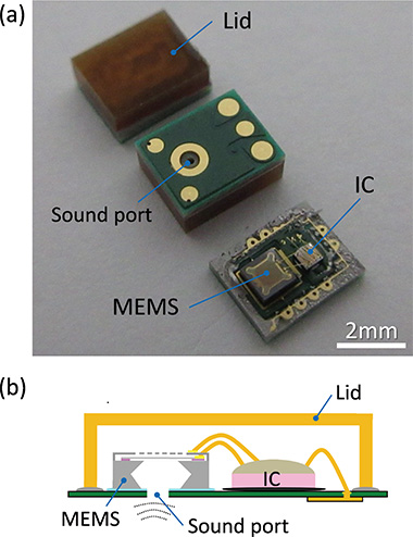
Fig. 1 shows the composition of a MEMS acoustic sensor module. A MEMS sensor chip for detecting sounds and an IC chip for signal readout are mounted on a substrate, which are covered with a lid. Fig. 1 (a) is a photo showing the external appearance of the MEMS acoustic sensor module with the lid opened, and Fig. 1 (b) is a schematic cross-sectional view. In the case of an acoustic sensor, the sound port on the substrate and the internal volume of the lid are important composing elements which have a decisive influence on the acoustic characteristics. In this figure, an evaluation module (2.95 × 3.76 × 1.25 mm) is shown.
2.2 MEMS acoustic sensor chip
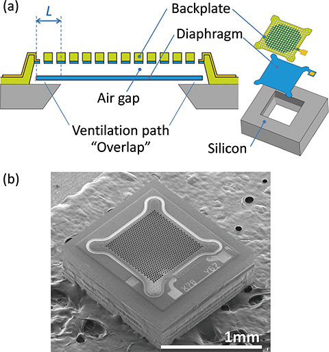
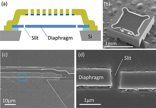
Fig. 2 (a) shows the structure of our conventional capacitance-type MEMS acoustic sensor chip 3). In this structure, a back plate with many openings (made of silicon nitride, 3.5 μm thick, and 750 μm on a side) and a square thin diaphragm (made of polysilicon and 0.8 μm thick) are facing each other with an air gap of 3–4 μm in between to form a capacitor. The vibration of the diaphragm caused by sound pressure is detected as a tiny variation in capacitance. As the Scanning Electron Microscope (SEM) image in Fig. 2 (b) shows, using MEMS technology enabled the size of the sensor to be decreased to within one millimeter, which is smaller than mechanical acoustic sensors.
In the acoustic sensor chip shown in Fig. 2 (a), there are small areas, shown as “L” in the figure, between the perimeter of the diaphragm and the silicon substrate where they are overlapping (hereinafter referred to as “the overlap,” which is 2.2 μm height and 60 μm width). These areas are the vent holes connecting the front side of the diaphragm with its rear side, which are important to prevent the characteristic change owing to the change of outside atmospheric pressure. However, if these areas are too large, sound diffraction occurs and the sensitivity is reduced. Therefore, the acoustic resistance needs to be high enough when the air passes through these spaces.
3. The noise source of the acoustic sensor
3.1 Noise problem with compact sensors
Not limited to acoustic sensors, a signal which is generated from inside an activated sensor module even if all inputs from outside are blocked is called “self-noise.” It is preferable that self-noise is low because it determines the minimum detectable limit. For compact sensors, the self-noise is more problematic, owing to the following three reasons:
- (1)
- Existence of noise generation mechanism specific to micrometer scale: Refer to the next section.
- (2)
- Deterioration of balance with IC noise owing to low sensitivity: If the sensing area is small, the sensitivity decreases and tends to be buried in IC-induced electrical noise (such as Johnson noise and flicker noise).
- (3)
- Noise resulting from small volume: In the case of an acoustic sensor, low frequency noise increases as the package volume decreases.
Therefore, the influences of the respective noises need to be taken into consideration when designing a sensor. The volume, which is Item No. 3, is dependent on the customer’s requirement, and for Item No. 2, the development of a low-noise IC for sensor is the key. In this study, we worked on the reduction of self-noise generated by a MEMS chip, described in Item No. 1.
3.2 Noise source specific to micrometer scale devices
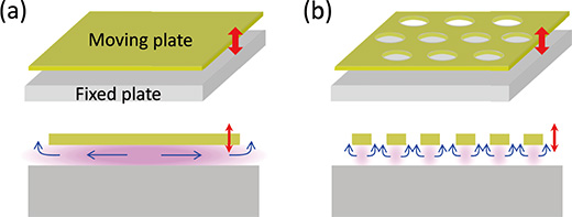
Micrometer scale structures become difficult to move owing to the influence of viscosity 4). A resisting force which prevents free movements acts on a plate which is placed several micrometers distant from a fixed plate and vibrates vertically. This phenomenon is called “squeeze film damping,” which is attributable to the fluid viscosity generated when a thin fluid layer between plates is pushed inside and outside the plates along the wall surface, as Fig. 3 (a) shows. Since this resisting force is inversely proportional to the cube of the distance between plates, it becomes very strong on micrometer scale 5). This damping resistance could be a significant noise source for MEMS devices, because the resisting force described above induces thermal fluctuation and the fluctuation shakes the diaphragm to become self-noise. Thermal noise is caused by thermal fluctuation of the air or structure, and the amplitude of the fluctuation is proportional to the square root of the resisting force 1). The MEMS acoustic sensor shown in Fig. 2 also has a area where the aforementioned squeeze film damping occurs at the overlap and at the air gap.
To reduce the damping resistance described above, the fixed plate or moving plate that has openings as shown in Fig. 3 (b) is generally used 5). However, it should be noted that making openings excessively causes a reduction in sensitivity.
3.3 Noise analysis based on an equivalent circuit model
It is known that the analysis based on an equivalent circuit model is effective for designing the sensor properties 6). Fig. 4 expresses the acoustic sensor module shown in Fig. 1 in an electro-acoustic equivalent circuit model, which shows the flow of the sound pressure which enters from a sound port and is then converted into an electrical signal through the elements corresponding to the respective MEMS structures and the IC. The overlap described in Section 2.2 is expressed by two resistive elements,
 and
and
 .
From this equivalent circuit model, the self-noise of the entire module can be predicted using a circuit simulator by adding both the IC-induced noise and the MEMS and package structureinduced noise. For details on how to calculate it, refer to the past report 7).
.
From this equivalent circuit model, the self-noise of the entire module can be predicted using a circuit simulator by adding both the IC-induced noise and the MEMS and package structureinduced noise. For details on how to calculate it, refer to the past report 7).
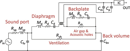
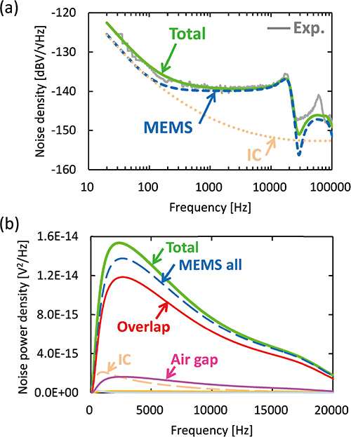
Fig. 5 (a) shows noise density spectra of our conventional acoustic sensor obtained through a simulation and an experimental result. The calculation result reproduces the actually measured spectrum shape well. In addition, in the midrange (100 Hz – 10 kHz), which is important for human auditory sensation, it is determined that MEMS-induced noise is more dominant than ICinduced noise. Fig. 5 (b) shows MEMS noise which is broken down into the resistive components in the equivalent circuit. Fig. 5 (b) shows power spectra of noise, which are weighted (A-weight) in a reflection of human auditory sensation. The area of each graph corresponds to the noise power. From this figure, it is determined that MEMS-induced noise consists mostly of the noise generated in the entire module (92% of all noise). The proportion of MEMS noise caused by the contribution of the damping resistance Rd at the overlap is overwhelmingly high (80% of the total), followed by the contribution of the damping resistance Rag at the air gap (11% of the total), and other contributions can be almost ignored.
3.4 Approach in noise reduction
The breakdown of noise factors clarified which part we should prioritize to work on the reduction of noise. The damping resistance in the narrow space is the major cause of self-noise generated in MEMS acoustic sensors, and we describe the reduction of damping below. First, we work on the reduction of the damping at the overlap, followed by at the air gap.
4. Proposal of a new low-noise structure
4.1 Slit diaphragm structure
As described in Section 3.3, the overlap is considered to be the major noise generation source. However, this overlap is necessary to diminish the impact of pressure change. Therefore, we propose a new diaphragm structure as shown in Fig. 6 (a) 7). In the structure, the perimeter of the diaphragm is separated by a narrow slit, and only the inner diaphragm surrounded by the slit vibrates under sound pressure. The advantage of this structure is that the damping between the diaphragm and the substrate can be eliminated completely because no silicon substrate is located anywhere facing the vibrating diaphragm (that is,
is zero). In addition, since the slit plays a role as a vent hole which connects the front side of the diaphragm with its rear side, designing the slit with a narrow width enables high acoustic resistance to be maintained.
(b) – (d) SEM images of the prototype MEMS chip
Figures 6 (b) – (d) show the SEM images of the slit diaphragm structure we developed 7). In the cross-sectional image, it can be confirmed that the diaphragm is separated by a slit of 0.5 μm width. To put this slit structure to practical use, the stability of the warpage of the diaphragm is important. This is because if the slit becomes misaligned in a vertical direction by 1 μm or more, the vent hole is enlarged and the sensitivity in the low frequency range decreases. Therefore, precise stress control of the polysilicon thin film which forms the diaphragm is required. By controlling key parameters such as the polysilicon film formation, ion implantation and annealing temperatures 8), we succeeded in stably maintaining the warpage of the diaphragm within +/− 0.5 μm over the whole 8-inch wafer surface.
4.2 Layout of narrow-pitch openings
If the overlap, which is the greatest noise source, is removed, the damping resistance in the air gap is the next dominant. In recent years, the damping resistance between a perforated plate with a regular honeycomb opening pattern and a fixed plate as shown in Fig. 3 (b) has been well researched and several analysis formulae have been proposed 9) 10). In this study, we calculated the damping resistance based on various combinations of a diameter
 and a pitch
 using the theoretical formula derived by Veijola 10). The damping resistance decreases as the opening ratio of the back plate increases. However, if the opening ratio is increased excessively, a reduction in sensing area causes a reduction in sensitivity and deterioration of SNR (signal-to-noise ratio). Therefore, we calculated the module SNR for the respective diameters and pitches in consideration of both sensitivity change and damping resistance change, as shown in Fig. 7 11). From our conventional product with a diameter of 17 μm and a pitch of 24 μm, it was determined that SNR could be improved further if the hole pitch and diameter are within the range enclosed by the white dotted line.
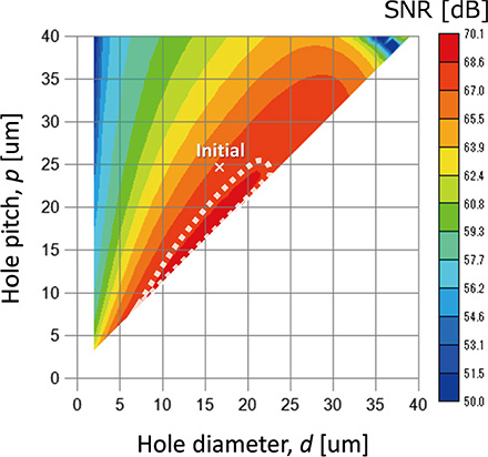
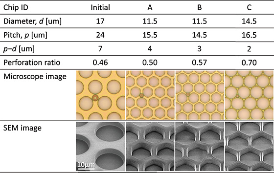
Therefore, we developed sensor chips equipped with a back plate for which the opening diameter and pitch are within the range enclosed by the white dotted line shown in Fig. 7. Table 1 shows the list of opening layouts. The slit diaphragm structure described in the previous section was applied to all layouts, and we only changed the layout of the openings in the back plate. Table 1 also shows the top views of the back plates we developd 11). Compared to the conventional product, the width
 ,
which shows the width of the remaining back plate between adjacent openings, is small. To realize narrow-pitch opening layouts like these, the stabilization of the etching process in which the openings are formed is the key. Controlling the photolithography and etching conditions so that the inclination angle of the wall surface approaches a vertical angle enabled the variation on the 8-inch wafer surface to be minimized even in the case of a narrow pitch where the remaining width was 3 μm or less.
,
which shows the width of the remaining back plate between adjacent openings, is small. To realize narrow-pitch opening layouts like these, the stabilization of the etching process in which the openings are formed is the key. Controlling the photolithography and etching conditions so that the inclination angle of the wall surface approaches a vertical angle enabled the variation on the 8-inch wafer surface to be minimized even in the case of a narrow pitch where the remaining width was 3 μm or less.
and microscopic and SEM images
5. Verification of noise reduction effect
5.1 Measurement method
We mounted the MEMS chip into which the new structures described in Chapter 4 were introduced as well as an IC manufactured by Omron on an evaluation module similar to the one shown in Fig. 1. In addition, we measured the sensitivity to a sound pressure of 1 Pa and the noise using a soundproof box. In the evaluation of narrow-pitch openings, we used a package with outer dimensions of 2.65 × 3.50 × 0.98 mm, which was more compact than the one shown in Fig. 1 (a). For the measurement, we used an audio analyzer (Audio Precision, SYS2722). Furthermore, to separate MEMS-induced noise from IC-induced noise, we also measured the noise when MEMS was replaced with a chip capacitor of equivalent capacitor.
5.2 Evaluation results
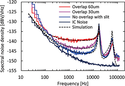
Fig. 8 shows the results of noise spectrum measurement conducted to examine the effect of the slit diaphragm structure 7). Compared to a conventional product (the overlap length is 60 μm), the noise floor around 1 k – 10 kHz decreased as the overlap length decreased, and the noise floor became even lower when the slit structure was applied. This fits with the prediction described in Section 3.3 that the major noise source in the midrange is the resistance of the overlap. As a result of applying the slit structure, we confirmed that the self-noise decreased significantly and the SNR of the module increased to over 66 dB, while that of the conventional module was 62 dB. Describing the result only, adopting a narrow slit width enabled the bandwidth to be broadened with no reduction in sensitivity to a lower range (< 20 Hz) than that of the conventional product. It was confirmed that adopting the slit structure is effective in broadening the bandwidth of frequency characteristics 7).
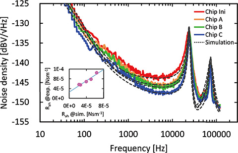
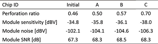
Next, Fig. 9 shows the noise spectra of the acoustic sensors with changed layout of openings on the back plate as described in Section 4.211). In all modules from A to C, it was determined that the noise floor around 1 kHz – 10 kHz was lower than that of the conventional layout and the noise decreased as the opening ratio increased. This fits with the noise breakdown calculation result described in Section 3.3, that the major noise source after removing the overlap was the air gap. As the inset in Fig. 9 shows, there was a good correlation between the measured damping resistance of the air gap and the theoretical calculation value. Table 2 shows the result of measuring sensitivity, noise and SNR of the module we developed. In all modules from A to C, the SNR was around 68.5 dB, which was improved by 1.0 dB or more than that of the conventional opening layout. It can be said that although increasing the opening ratio of the back plate reduces the sensitivity, the noise reduction effect is dominant in modules A–C, which resulted in the improvement of SNR 11). Considering the balance with the mechanical strength of the back plate, we finally chose the opening layout of module B.
(Inset) Comparison of the resistance in the air gap between calculation value and
actual measurement value
5.3 Summary of noise reduction effect
As we described in the previous section, introducing the slit diaphragm structure as well as optimizing the opening layout of the back plate enabled the self-noise of the acoustic sensor to be reduced to one-fourth (equivalent to −6 dB).
6. Conclusions
We introduced new structures for suppressing the major noise sources in a MEMS acoustic sensor to realize a compact and high-performance acoustic sensor. We succeeded in reducing the self-noise of the sensor by 6 dB compared to the conventional sensors and achieving SNR of 68 dB, which was the highest level in the world as a MEMS acoustic sensor as of 2018. The fact that the noise was reduced by 6 dB means the signal quality can be maintained if the distance between the sensor and the sound source was doubled, which is advantageous in obtaining clear acoustic data. The acoustic sensor we developed this time is expected to be utilized in new acoustic sensing applications such as equipment abnormality detection or biological sound detection, by taking advantage of its characteristics which are small size, low noise and wide band.
In addition, the method of breaking down the noise sources in a quantitative way using an equivalent circuit model can be applied to a wide variety of applications other than acoustic sensors in order to systematically reduce the noise. In particular, we can say that controlling air damping is the common issue when designing MEMS devices equipped with micrometer-order driving parts and this method can be effectively referred to.
Finally, the practical realization of the new structures we introduced this time (slit diaphragm structure and narrow-pitch opening layout) is the result of the maturation of production technologies such as the control of polysilicon thin film stress and in-plane etching stability. It can be said that the effort we made in this development is an example of best practices showing how collaboration between design technology and process technology is important for MEMS devices.
Acknowledgements
This development was conducted with the support of Mr. Takafumi Ota, Mr. Kenta Kajikawa and the employees of the Yasu Plant who cooperated in the fabrication of prototype wafers and process improvement. We would also like to thank Mr. Takashi Fuchimoto and Mr. Takuya Katagiri, who belong to the Development Department III and cooperated in the mounting of packages, the employees of the Quality Assurance Division who cooperated in the observation of SEM, and the microphone development members who provided much valuable advice. We would like to take this opportunity to express our sincerest gratitude.
References
- 1)
- T. B. Gabrielson: “Mechanical-thermal noise in micromachined acoustic and vibration sensors”, IEEE Transactions on Electron Devices, 1993, Vol. 40, p. 903-909.
- 2)
- M. Boustany and J. Bouchaud: “Adoption of high-quality microphones promises revenue growth”, IHS technology’s report, 2014.
- 3)
- T. Kasai, Y. Tsurukame, T. Takahashi, F. Sato, and S. Horiike: “Small silicon condenser microphone improved with a backchamber with concave lateral sides”, in Digest Tech. Papers Transducers 2007 Conference, 2007, p. 2613-2616.
- 4)
- S. D. Senturia.; Microsystem Design, Kluwer Academic Publishers, 2001, 689 p.
- 5)
- Z. Škvor: “On the acoustical resistance due to viscous losses in air gap of electrostatic transducers”, Acoustica, 1967, Vol. 19, p .295-299.
- 6)
- S. C. Thompson, J. L. LoPresti, E. M. Ring, H. G. Nepomuceno, J. J. Beard,W. J. Ballad, and E. V. Carlson: “Noise in miniature microphones”, J. Acoust. Soc. Am., 2002, Vol. 111, p .861-866.
- 7)
- T. Inoue, A. Murakami, Y. Horimoto, Y. Uchida, and T. Kasai: “Design of an advanced microphone with high SNR and flat frequency response using equivalent circuit model”, Proceedings of the 8th JSAP integrated MEMS symposium, 26am1-D-1, 2016.
- 8)
- Tomohiro Yoshimura: “Predictive Control by Whole Process PLS Model in MEMS Fabrication”, AEC/APC Symposium Asia 2015, MC-O-23, 2015.
- 9)
- M. Bao, H. Yang, Y. Sun, and P. J. French: “Modified Reynolds equation and analytical analysis of squeeze film air damping of perforated structures”, J. Micromech. Microeng., 2003, Vol. 13, p .795-800.
- 10)
- T. Veijola: “Analytic damping model for an MEM perforation cell”, Microfluidics and Nanofluidics, 2006, Vol.2, p .249-260.
- 11)
- T. Inoue, Y. Uchida, K. Ishimoto, and Y. Horimoto: “Optimized design of squeeze-film damping toward high SNR MEMS microphone”, Proceedings of the 34th Sensor Symposium on sensors, micromachines and applied systems, 01am1-A-4, 2017.
The names of products in the text may be trademarks of each company.