


Efforts to Improve the Accuracy of Board Appearance Inspection by Using a Multi Direction Imaging Method and Automatic Optimization of Inspection Criteria
- Multi-CH Lighting
- Visual Inspection
- Programming Automation
- Optimization
- 3D Recognition
The wetting inspection of solder on components is the most important part of the board appearance inspection. However, solder forms various shapes because of the shape of electrodes, pads, and land. In addition, it is difficult to correctly measure the solder shape due to phenomena, such as shadows, and secondary reflections caused by the board design and various surrounding components. In addition, even if the solder shape can be captured correctly, it is necessary to combine the measured values at various points in order to set the inspection criteria for determining good and bad solder. In this paper, we propose a method for automatically determining the inspection criteria by using a hardware structure for the lighting and camera imaging systems that accurately captures solder wettability and eliminates the effects of design constraints, such as secondary reflections and shadows, and a combinatorial optimization method. As a result of verifying the effectiveness of the proposed method, it was found that the proposed method improved the correctness of the inspection criteria by 4.9% and the incorrectness of the inspection criteria by 3.4% compared to the conventional method.
1. Introduction
Our Inspection Systems Division has solution operations centered around the automatic optical inspection (AOI) business for PCB mounting processes and serves customers to solve their quality challenges. Our AOI inspection system is based on equipment technologies, including mechanical, electrical, and optical measurements and inspection algorithms, and the so-called teaching, in other words, the setting of the screening criteria for the acceptability of items subject to inspection. From among these technologies, a combination has been made of an optics core technology known as color highlight lighting and a 3D inspection technology based on the recent mainstream phase shift method. This combination allows more accurate inspection of components’ attitudes and positions or solder shapes than before. At present, however, situations often occur where correct measurement is impossible because of optical phenomena, including shadows of other components caused by board design factors, such as component mounting positions, and secondary reflections from oppositely positioned components (e.g., cases where optical information is unavailable or unreliable). In such cases, alternative methods, such as 2D inspection, are employed, which, however, not only leads to an increased number of settings items and hence an increased teaching workload but also requires inspection imaging-related knowledge and image adjustment skills. As a result, the post-installation cost poses a more serious problem than the cost of equipment (for example, a teaching logic used to determine the acceptability of solder based on the solder wetting angle needs to be combined with not the optical information of some solder but the information of distinctive surrounding solder).
Moreover, teaching operators are difficult to retain. Consequently, inspection programs cannot be guaranteed for quality, and inspection systems cannot be exploited to the fullest of their performance, resulting in the problems of false-positive calls (non-defectives erroneously determined as defective by the system) and false-negative calls (defectives erroneously determined as non-defective by the system).
This paper proposes an improved lighting system configuration for components subject to inspection and improvements to inspection-criteria determination logic.
2. Conventional Technologies
A 3D shape measurement method based on the color highlight method1) is well known in technical fields, where components mounted on printed circuit boards are inspected for the condition of solder joints. This method is a technology invented by Omron and is the de-facto standard method in today’s AOI color inspection.
Fig. 1 schematically illustrates the configuration and principle of a color highlight system. The color highlight lighting system has three elevation angle levels (upper, medium, and lower) and is built to apply red light from the upper level, green light from the middle level, and blue light from the lower level. Besides, the lighting system has an imaging unit (camera) installed at its center. With the red, green, and blue beams of light from the respective levels being reflected to the angle normal line at each solder position, color features will emerge (as the hues of the light source in the specular reflection direction as viewed from the camera). Under this condition, image pickup operations are performed to turn the three-dimensional shape of the solder surface into two-dimensional color information.
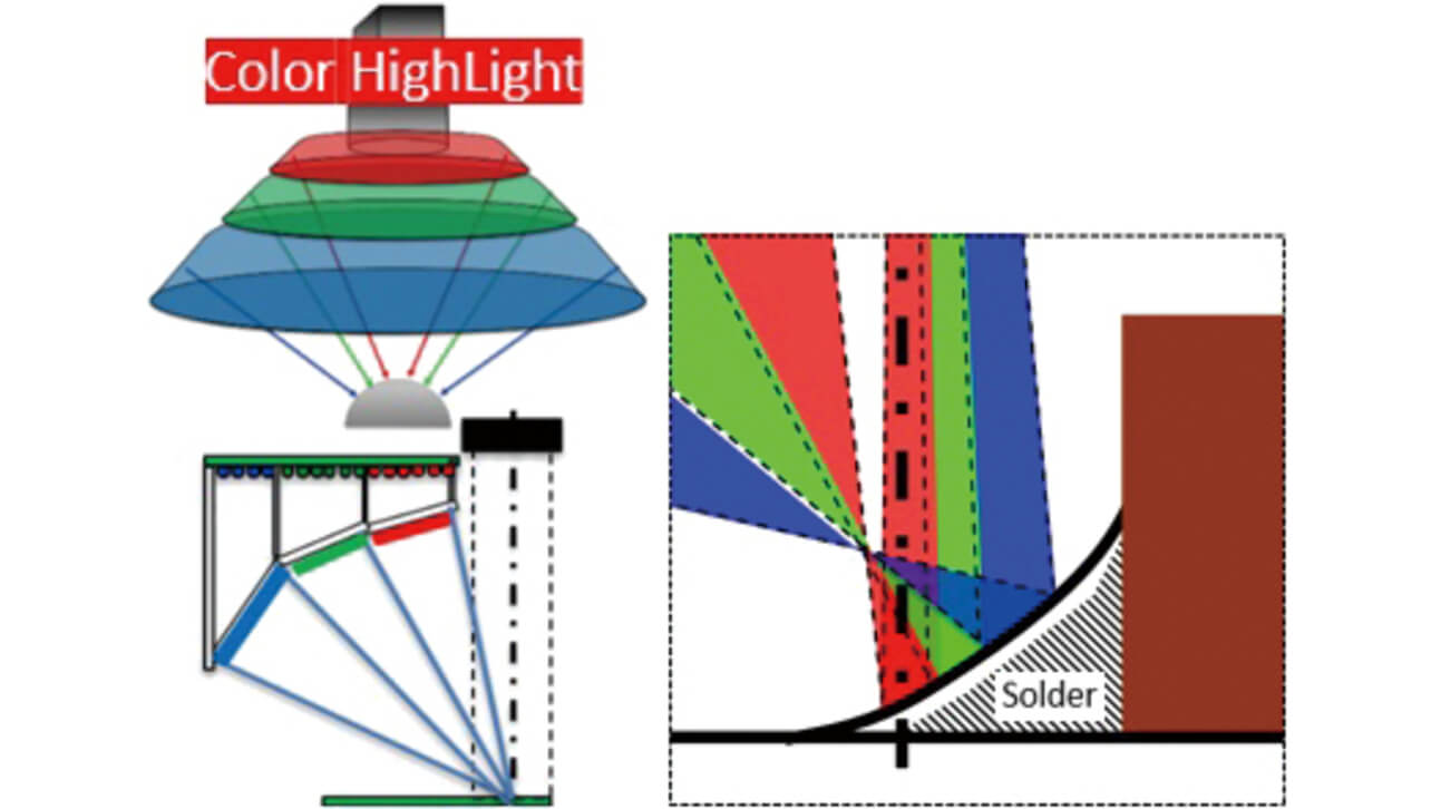
The measurement accuracy for tilted solder surfaces is measurable as two-dimensional hue information with a certain degree of accuracy. However, when the lighting system radiates light in all directions, divisions cannot be made between angle normal lines. Hence, no distinctions can be made between tilts with the same angle. More specifically, it becomes difficult to determine whether the solder surface tilt builds up relative to the electrode (the so-called upward wetting condition) or extends lower than the electrode (the so-called non-wetted condition). In other words, as long as the light is radiated from 360 degrees around, the problem persists that directions are impossible to differentiate based on two-dimensional hue information.
Accordingly, Omron has combined its AOI (VT-S Series) with the 3D shape measurement of diffusing objects by the phase shift method, as shown in Fig. 2, independently of the 3D shape measurement of specular objects by the above-mentioned color highlight method, to measure heights more accurately, thereby enabling the reconstruction and measurement of solder shapes2).
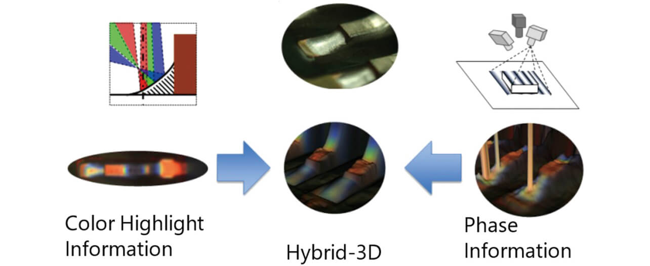
Incidentally, the phase shift method is one of the techniques that analyze the distortion of structured light patterns projected on the surface of an object to reconstruct the three-dimensional shape of its surface. This technique complementarily solves the challenges in each conventional method and serves as a method of handling fluctuations in the gloss or shape of solder surfaces.
However, even this phase shift method has the following problems: correct measurement is difficult near an electrode where supposedly obtainable phases are shifted due to secondary reflections from the end faces of the electrodes; or measurement is impossible, in principle, in the case of highly specular solder surfaces, from which projected stripe patterns do not return to the camera.
Besides, the distinction between non-defectives and defectives under inspection requires establishing inspection criteria for defective/non-defective determination based on what portion of the solder has what shape. Therefore, without correctly establishing inspection criteria, false-positive or false-negative calls will occur even if solder shapes are correctly reconstructed.
3. Solution
This section presents a fundamental revision made of the hardware structure and a combinatorial optimization method employed to automate inspection criteria setting to solve the three challenges of (i) identifying solder orientations, (ii) eliminating shadows/secondary reflections, and (iii) making inspection criteria setting non-skill dependent.
3.1 Directional Lighting (MDMC Lighting)
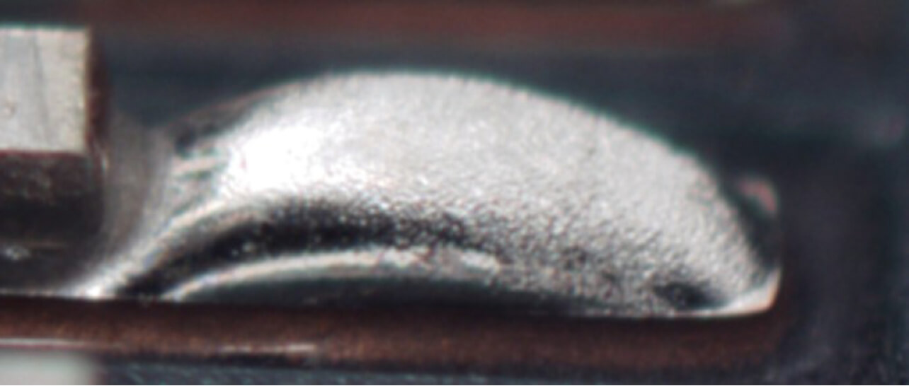
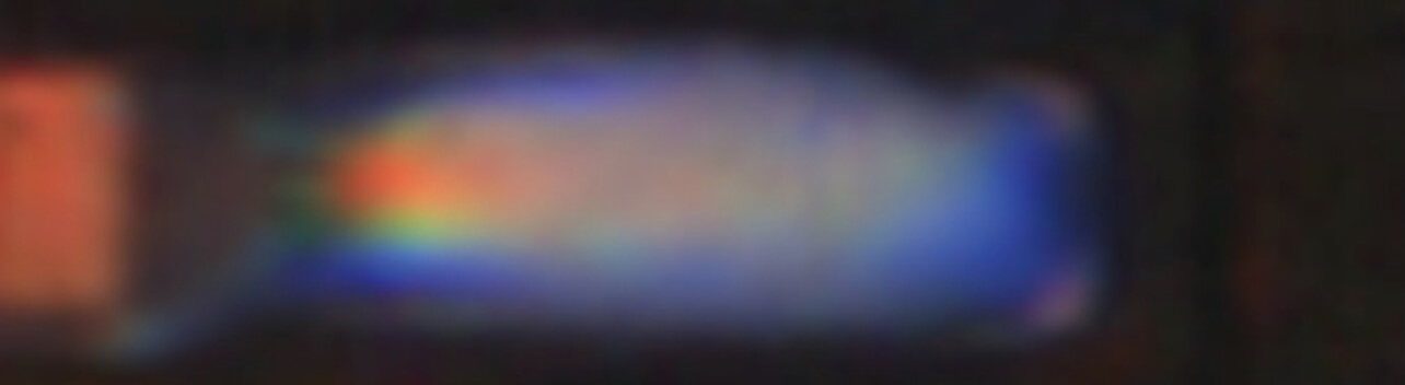
When captured by the color highlight method, non-wetted solder, such as that in Fig. 3, would look like the image shown in Fig. 4. This method can represent gently tilted solder areas in red and steeply tilted areas in blue. However, a closer look at the image reveals that two solder areas with similar normal angles are similarly rendered in red regardless of the wetting direction. Hence, solder orientations are difficult to identify. This problem occurs because there is no identifying whether the irradiation light is incident from, for example, a 0-degree direction or a 180-degree direction when radiated from all directions (360 degrees). Therefore, the color features and positions of surrounding solder must be considered to break down optical information and perform teaching.
Hence, we developed a configuration for obtaining highly reliable optical information by dividing optical information not after but during image pickup.
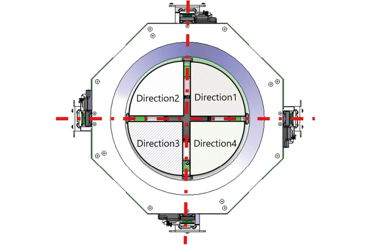
The conventional 360-degree all-around color-highlight lighting system configuration was divided into four quadrants from the first to the fourth as shown in Fig. 5 to provide a multi-direction multi-color (MDMC) lighting system configured to apply light in four directions, each 90 degrees apart.
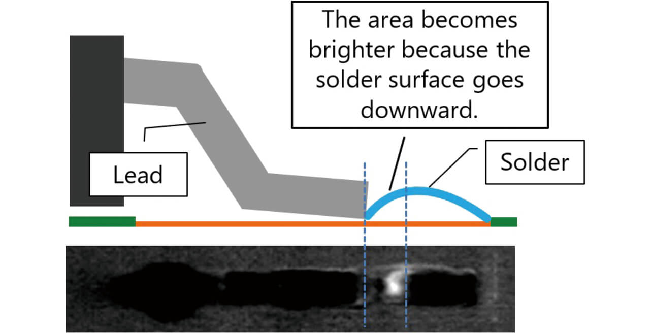
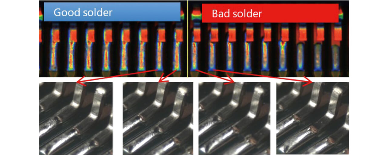
Next, Fig. 6 shows two images of solder under directional lighting. These images show the solder irradiated with light from the front and back faces of the electrode to its tip, respectively. The surface tilted toward the irradiation direction appears bright.
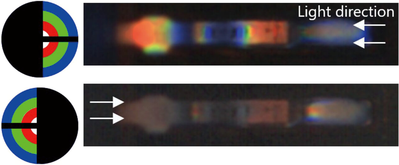
Fig. 7 shows a differential image based on the two images of solder under directional lighting from Fig. 6. This image shows high-brightness spots intensely irradiated with light from the back face, which suggests a high possibility that the solder wetting direction was downward.
3.2 Quad-Directional Light Projector
The phase shift method is an algorithm that uses optical information from certain structured light pattern projections. Because shadows always occur when light is projected from one direction, this method also requires optical information from the opposite direction. Besides, considering that projected light reflected on the side faces of components becomes a noise factor, we adopted a configuration for projecting light from four mutually opposite directions, left and right and front and back, to obtain highly reliable optical information.
3.3 Optimization of Inspection Criteria
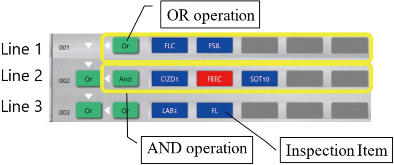
Typical inspection items in solder inspection include the wetting height and wetting angle for the electrode and the wetting length and wetting angle for the land. Fig. 8 shows the screen for setting inspection criteria for determining the acceptability of sites under measurement.
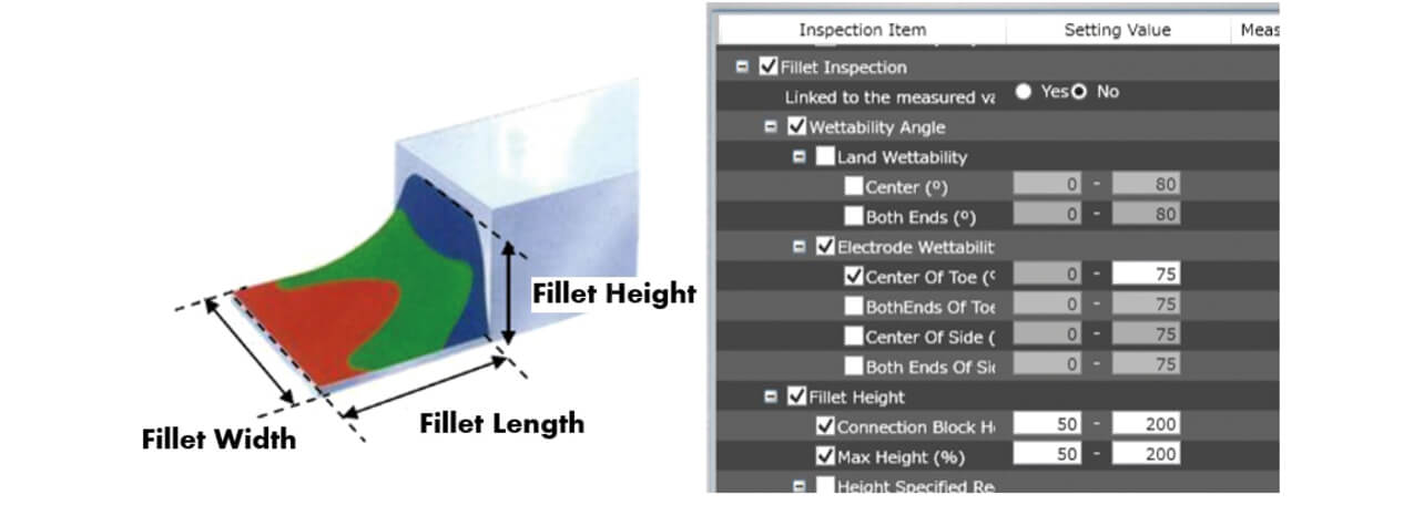
Each of these inspection items requires setting the inspection criteria for the upper and lower limits. It is relatively easy to determine inspection criteria for one inspection item. In practice, however, acceptability decisions cannot always be made based on a single inspection item but often needs to be made comprehensively using logical sums or logical products obtained by combinations of multiple inspection items (Fig. 9). The reason is that solder under inspection may assume various shapes depending on various fluctuation factors, such as the electrode shape, the land design, or the ingredients of the solder.
However, it takes numerous combination calculations to determine the inspection criteria that best suit multiple inspection items and combinations. Setting optimum inspection criteria manually requires much time and experience, which pose an extremely difficult task. This subsection considers the optimization of inspection criteria.
The following shows the workflow leading up to the determination of inspection criteria:
- (i) Writing out measured values
- (ii) Clustering
- (iii) Developing logical expressions
- (iv) Calculating the evaluation value
- (v) Selecting the inspection reference values
In Step (i), measured values are obtained as the outputs from the respective inspection items. The assumption here is that the measured values from defectives are manually labeled as defective.
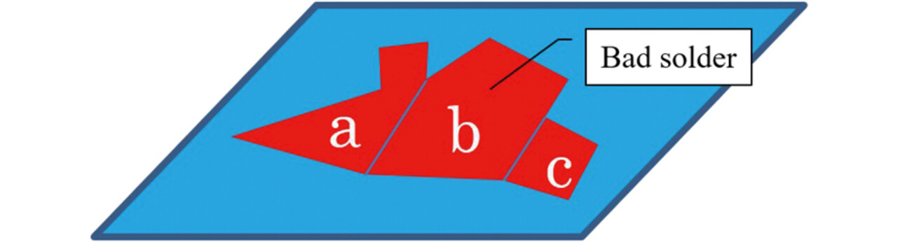
Then, in Step (ii), clustering is performed on the measured values of various defective shapes, including lifting, non-wetting, and excessive or insufficient solder. The k-means++ method3) is used for clustering. In this way, defects more or less similar in shape are grouped into single defect clusters (Fig. 10).
Then, in Step (iii), the most efficient inspection item and logical expression for detecting individual defect clusters are identified. The superlative “most efficient” is used here to describe a logic that produces the least number of false-positive calls when all the items in, for example, Cluster “a” are determined as defective (this logic is referred hereinafter to as a first logic).
First, the first logic for each cluster, the most efficient logic, is selected as in Fig. 11.
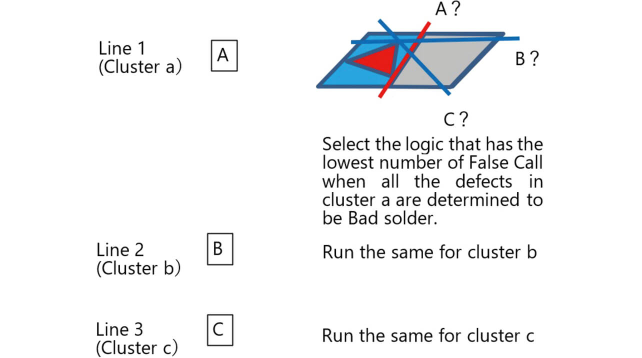
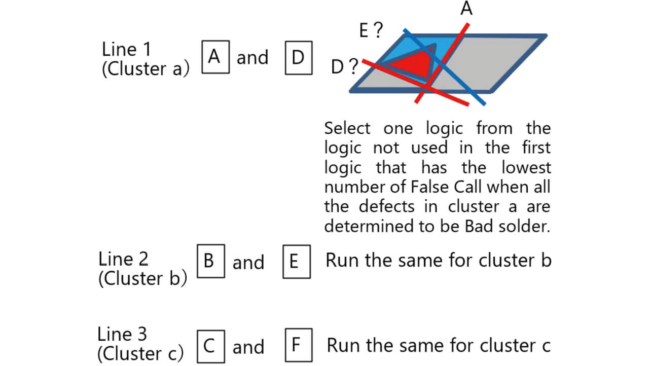
Next, each remaining logic not selected as a first logic is combined with the first logic for one of the clusters into a logical product. The logical product thus obtained is the second logic for the cluster that includes the least number of false-positive calls when the inspection criteria are set within a false-negative call-free range (Fig. 12). The same is repeated for each remaining logic to develop logical expressions.
In Step (iv), for each line of each logical expression, the value range settable as an inspection criterion is divided into 20 subranges (set in 5% increments, e.g., 0%, 5%, 10%…95%, 100% if settable in a 0% to 100% range) to calculate the number of false-positive or false-negative calls for each applicable inspection criterion.
Then, the evaluation value is defined as follows:


- NGood : Number of OK calls made
- NBad : Number of NOK calls made
- MN : number of false-negative calls
- MP : number of false-positive calls
Then, a ranking is made of the top-50 inspection criteria combinations having a high evaluation value for each logical expression.
In Step (v) (Selecting the inspection reference values), the following rules apply to select the logical expression from among the logical expression candidates obtained by the ranking calculation:
- If any defect is detectable only from a specific line, adopt the candidate corresponding to the defect.
- If a defect is detectable with more than one candidate, select the one with a higher evaluation value.
- If all defects become detectable halfway through the process, select the candidate with the least number of false-positive calls for the subsequent lines.
- If more than one candidate exists with an equal number of false-positive calls, adopt the one with the largest margin (inner).
The above rules allow the selection of combinations with fewer false-positive and no false-negative calls.
4. Empirical Results
4.1 Directional Lighting
For a sample of 0.5 mm pitch quad flat packages (QFPs) with the solder wetting angle gradually changing relative to the electrode, we investigated the identification accuracy for solder normal lines (orientations) (Fig. 13).
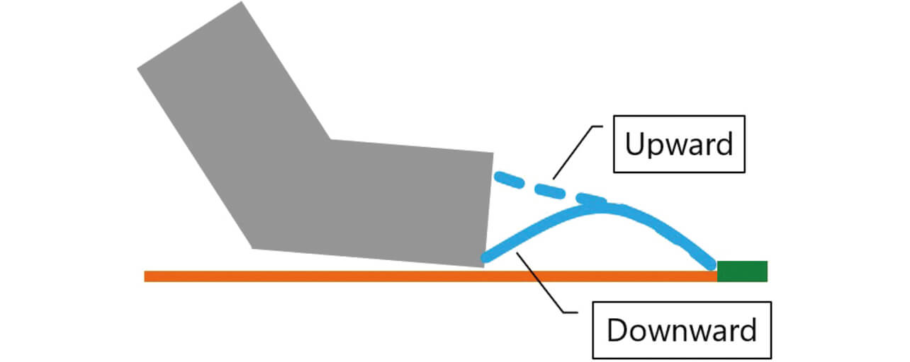
Fig. 14 shows the external views and color-highlight images of inspected components. Table 1 shows the breakdown of the evaluation sample size. Note that non-defectives and defectives were sorted apart by a skilled operator using a digital microscope.
| Sample size | |
|---|---|
| Non-defectives | 464pins |
| Defectives | 832pins |
Table 2 shows the results of comparing the binary accuracy for non-defectives and that for defectives before and after improvement.
| Results | Binary accuracy for non-defectives |
Binary accuracy for defectives |
|---|---|---|
| Before improvement | 87.3% | 94.8% |
| After improvement | 97.2% | 100% |
Regarding the identification accuracy for solder normal lines (orientations) by conventional color-highlight images, the binary accuracy for non-defectives was 87.3%. Meanwhile, the value improved to 97.2% when the images of solder under directional lighting were used. The binary accuracy for defects also improved from 94.8% to 100%, which confirmed a significant improvement effect for both non-defectives and defectives.
4.2 Quad-Directional Light Projector
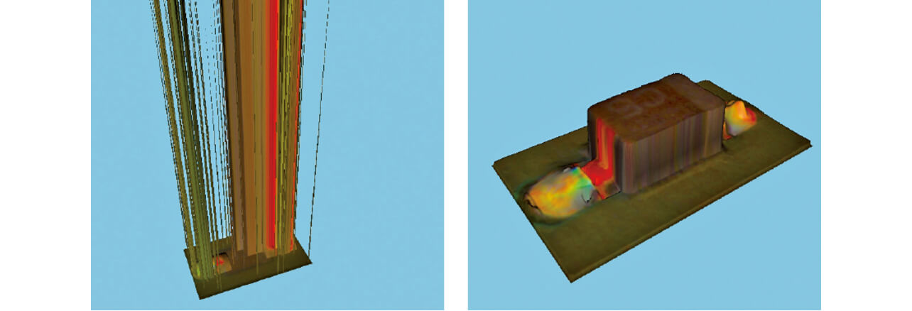
We confirmed the improvement effect for components that cast shadows due to adjacent components. While Fig. 15 shows a typical component layout of such components, Fig. 16 shows the bird’s-eye-view images before and after improvement. With bidirectional light projection, the projected light was blocked by adjacent components and failed to reach the component of interest, resulting in an inaccurately reconstructed shape. Meanwhile, with quad-directional light projection, the projected light correctly fell on the surfaces of the component, resulting in an accurately reconstructed shape.
4.3 Optimization of inspection criteria
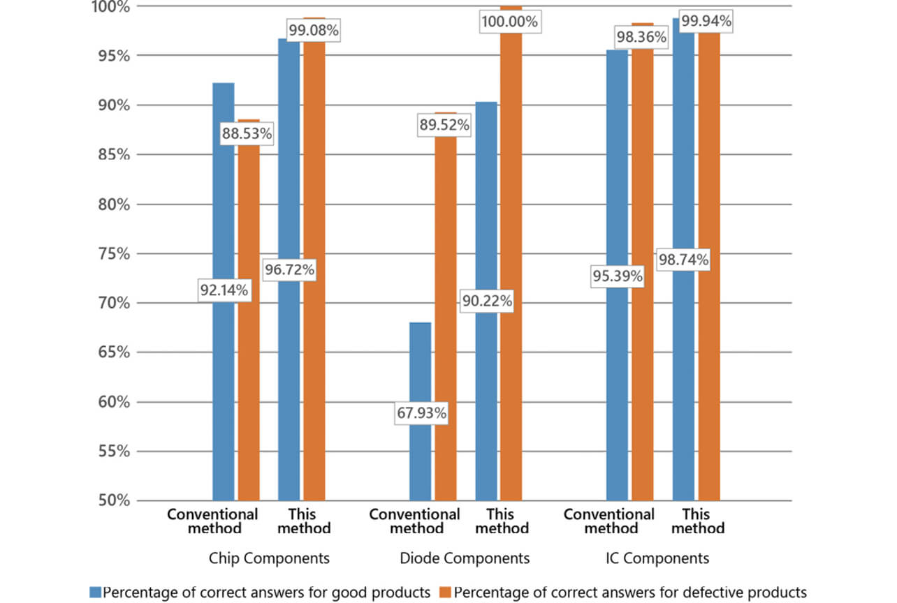
For three typical types of components, chip components, diode components, and IC components, we used the conventional method and the one proposed here to compare the binary accuracy for non-defectives with that for defectives. Table 3 shows the breakdown of the sample size of pins subject to evaluation. The conventional method meant here was the one manually set up by a skilled operator based on his experience. The defects of evaluation interest were wetting defects. Regarding defective/non-defective determination, the skilled operator labeled the pins beforehand so that non-defective pins determined as non-defective or defective pins determined as defective by the inspection machine would be counted as correctly inspected pins.
| Number of non-defective pins |
Number of defective pins |
|
|---|---|---|
| Chip component | 3233 | 218 |
| Diode component | 43916 | 229 |
| IC component | 478216 | 1707 |
Fig. 17 shows the results of the comparison in terms of binary accuracy. The binary accuracy for both non-defectives and defectives improved for all three component types. The method proposed here improved the average binary accuracy for non-defectives among all component types by 4.9% and that for binary accuracy for defectives by 3.4%, compared with the conventional method.
5. Conclusions
To solve the traditional challenge of accurately determining the acceptability of wetted solder, we developed an imaging system for direct observation of solder orientations and successfully improved the reconstruction accuracy for solder shapes. Then, we added a quad-directional light projector that significantly reduced the occurrence probabilities of shadows and secondary reflections to allow inspection with lower-noise images closer to real shapes.
Besides, the traditional stumbling block for operators other than those skilled in teaching, in other words, the task of establishing the inspection criteria for defective/non-defective determination based on what portion of the solder has what shape, was automated by the optimization of inspection criteria and made performable without reliance on personal skills.
Next, we intend to provide a method of quantitatively evaluating mounting processes in terms of process capacity through quantitative measurement of solder shapes besides simplistic non-defective/defective determination. Such a method will allow quick identification of mounting process issues, thereby leading to improved mounting processes and even improved board designs and will provide a new added value of reducing inspection cost and overall quality cost to maximize customer satisfaction.
References
- 1)
- Japanese Examined Patent Publication No. 6-1137 (Kokoku)
- 2)
- S. Raschka and V. Mirjalili, Python Machine Learning - Python Machine Learning Programming Wizard, the theory and the practice with data science, 2nd Ed. (Japanese version translated under the supervision of S. Fukushima), Tokyo, Japan: Impress (in Japanese), 2018, pp. 336-337.
- 3)
- T. Sugiyama, M. Kishimoto, S. Fujii, and S. Sugita, “SJI (Solder-Joint-Inspection) 30 Years and Issues to Be Solved Based on 3D Technology,” in Proc. 31st JIEP Spring Lecture Conv., 2017, pp. 70-73.
The names of products in the text may be trademarks of each company.