


Solder Vibration Printing Technology that Enables Mixed Mounting from 0402 to Large Components
- Surface mount
- Solder paste printing
- 0402M
- Ultrasonic vibration
- High aspect ratio
The size of passive components mounted on boards composing a product has been decreasing. Mainstream size will be 0603 (0.6 × 0.3 mm) and 0402 (0.4 × 0.2 mm), whereas the conventional sizes are 1608 (1.6 × 0.8 mm), 1005 (1.0 × 0.5 mm). In order to use this part with FA equipment, it is essential to be mixed with large components. In mounting various components dimensions, it is necessary to accurately supply solder that electrically connects the components and the board pattern from the one required for large components to a small amount, such as 0402, on the board. For this reason, solder characteristics, stencil surface processing, PWB pattern dimensions, and vibration printing technology were evaluated in order to supply solder with a high aspect ratio by the printing method. Printing with an aspect ratio of 2.7 (stencil thickness 0.12 mm, opening size Φ 0.18 mm) is realized. For that purpose, we searched for the effects of material extraction and vibration printing technology. As a result, we were able to exceed the previous1) 2.4, and achieved a volume ratio Cpk 1.80 of 2.7.
1. Introduction
As part of the recent trends in industrial products, electronic devices are undergoing functional and added-value enhancement through the addition of communication functions or AI processing functions or the expansion of data processing capacity. Accordingly, printed wiring boards constituting parts of the electronic devices are becoming smaller but more densely mounted with an increasing number of components. As a result, surface-mount components are becoming smaller in size. Size- 0603, Size-0402, or even further smaller components are forming the mainstream2). For FA equipment, mixed mounting is required of differently sized components ranging from Size- 0402 components to large components, such as connectors. One of the challenges to mixed mounting is the stabilization of high aspect ratio solder printing. Hence, the previous paper presented our efforts made to achieve stable solder printing at an aspect ratio of 2.4.
The present paper reports on our efforts made to achieve a target Cpk* of 1.80 for an aspect ratio of 2.7 (*process capability index for print results, represented as the volume ratio with the upper and lower references set to 170% and 50%, respectively). During our efforts for vibration printing, we took measurements of actual vibration phenomena to evaluate the relationship between vibration amount and printability.
2. Challenges to high aspect ratio solder printing
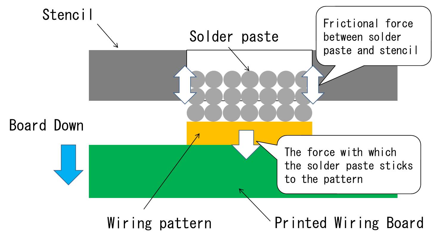
In solder printing, solder paste (hereafter “solder”) is fed (hereafter “filled”) into stencil apertures, followed by the lowering of the printed wiring board (hereafter “PWB”) to transfer the stencil aperture-shaped solder onto the electrode pattern. Successfully stable printing depends on the balance between the solder adhesion force to the PWB electrode pattern and the frictional force between the stencil and the solder (hereafter “shear stress”) arising from the solder adhesion to the stencilʼs aperture inner wall during the lowering of the PWB (hereafter “stencil separation”) as shown in Fig. 1.
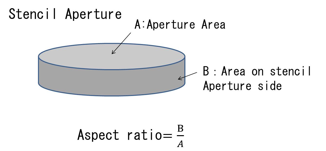
These forces are proportional to the solder contact area. The ratio of this area is expressed as an aspect ratio (see Fig. 2). In solder printing technology, the aspect ratio is an important factor. It is known that an increase in this value leads to reduced printability3). An increase in stencil-solder contact area compared to the PWB-solder contact area leads to higher shear stress due to which solder residue likely occurs in the stencil apertures, reducing the volume of solder transferred to the PWB. Stencil thickness reduction is an effective method of reducing the aspect ratio. In the case, however, of a PWB mounted with a mix of components highly variable in lead height, such as connectors, solder is insufficiently filled in for these components, giving rise to the problem of reduced bonding strength. Hence, stencil thickness reduction is not an option for the printing of small components. The mainstream soldering stencils for FA equipment PWBs are 0.12 mm thick.
Then, an aspect ratio of 2.4 applies when printing with the aperture area for Size 0402.
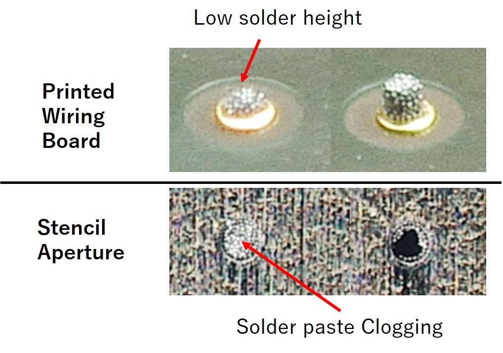
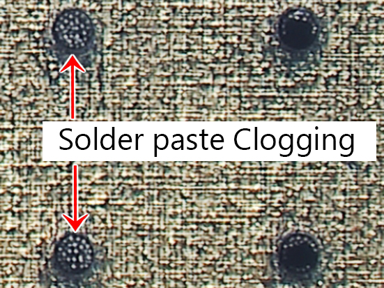
Last time, we measured the viscoelastic properties of solder using a rheometer and optimized the stencil separation speed to reduce shear stress. These activities brought to our attention the importance of optimizing the printing conditions, such as stencil surface coating and stencil separation control, suitably for the properties of the solder. Meanwhile, an increase in the aspect ratio to 2.7 led to a reduced solder height and more stencil apertures clogged with solder as shown in Fig. 3. The likely cause was the failure of the solder to come into good contact with the PWB pattern, resulting in an insufficient solder adhesion force to the PWB. To address this problem, we evaluated the relationships between the properties of solder and the stencil surface coating and between the PWB pattern size and the stencil aperture size, and the effectiveness of our method of solder vibration printing.
3. Evaluation of the influences of solder, stencil surface coatings, and PWB pattern designs on printability
3.1 Content of the evaluation
The solder used was Solder A, which was newly put under evaluation this time, and Solder B, which had been used last time. A hydrophilic (lipophilic) coating and a water-repellent (oil-repellent) coating were used as stencil surface coatings for evaluation of the frictional force with the solder. The PWBs used were each printed using a solder resist thinner with the copper foil and a stencil aperture size larger than the PWB pattern size to ensure tighter adhesion between the stencil and the pattern. Tables 1 and 2 show the specifications for the solder and the PWB, respectively. Table 3 shows the relationship between the PWB pattern sizes and stencil aperture sizes of interest.
| Solder | Particle size | Viscosity (Pa·s) | Flux content (Wt%) |
|---|---|---|---|
| A | 20 to 38 μm | 117 | 11.5 |
| B | 10 to 15 μm | 183 | 11.5 |
| Item | Descriptions |
|---|---|
| Dimensions (mm) | 115 × 180 × 1.6 t |
| Pattern size (mm dia.) | ϕ0.16, ϕ0.18, ϕ0.20, ϕ0.22, ϕ0.24, ϕ0.26, ϕ0.28, ϕ0.30, and ϕ0.32 |
| Solder resist thickness | 25 μm |
| Copper foil thickness | 35 μm |
| Surface treatment | Electroless thin Au plating |
| Silkscreen | N/A |
| PWB of interest | Pattern size (mm) | 0.20 | 0.22 | 0.16* | 0.18* | |
|---|---|---|---|---|---|---|
| Stencil | Aperture size (mm) | 0.16 | 0.18 | 0.16 | 0.18 | |
| Target aspect ratio for datum surface | PWB | 3.0 | 2.7 | 3.0 | 2.7 | |
| Squeegee | 2.8 | 2.5 | 2.8 | 2.5 | ||
* In these cases, the PWB pattern and the stencil aperture were the same size (conventional designs).
3.2 Conditions of the experiment
Table 4 shows the printing conditions used for the evaluation. To eliminate the influence of PWB warpage when solder printing, we used the PCB vacuum-suction function of the stencil printer to make corrections during printing so that each PWB provided a flat surface. The print results were examined by a solder paste inspection machine (CKD-built VP-6000M) to quantify the resist opening pattern. For each experimental condition, the stencil underwent cleaning to eliminate the influence of the solder residue adhering to it. Each PWB was evaluated for printability based on the data of the stably printed last six sheets (Sheets 3 to 8) from among the eight PWB sheets printed.
| Stencil printer | Panasonic-built SP-60 |
|---|---|
| Squeegee blade | Metal (10-mm protruding margin) |
| PCB support | Solid jig, dedicated vacuum suction box |
| Squeegee speed | 50 mm/sec |
| Squeegee pressure | 35×10−2N |
| Attack angle | 60° |
| Print gap | −0.2 mm |
| Stencil separation speed | Constant velocity: 10 mm/s |
| Stroke: 3 mm | |
| Bottom support first | |
| Waiting time before stencil separation | 0 |
3.3 Evaluation results
Table 5 shows the volume ratio Cpk values for each pair of solder and stencil of interest. Regardless of the stencil surface coating and the aspect ratio, higher Cpk values were observed for Solder A than Solder B, indicating the superiority of Solder A to Solder B. When the aspect ratio was above 2.7, regardless of the solder, higher Cpk values were observed with the hydrophilic stencil surface coating than with the water-repellent one.
Table 6 shows the volume ratio Cpk values for the aspect ratio of 2.7. These results reveal that, regardless of the solder, higher Cpk values were obtained with the PWB pattern size larger than the stencil aperture size.
A volume ratio Cpk of 0.87 was achieved by printing with the optimal combination of the above factors.
| Design aspect ratio | |||||
|---|---|---|---|---|---|
| Solder | Stencil | 3.0 | 2.8 | 2.7 | 2.5 |
| A | Water-repellent coating | 0.14 | 0.18 | 0.69 | 1.47 |
| Hydrophilic coating | 0.23 | 0.34 | 0.87 | 1.90 | |
| B | Water-repellent coating | 0.00 | 0.00 | 0.21 | 0.54 |
| Hydrophilic coating | 0.00 | 0.00 | 0.26 | 0.39 | |
* Specification: 50% < printing volume < 170%
| Solder A | Solder B | |||
|---|---|---|---|---|
| Dimensional relationship |
PWB pattern size = stencil aperture size |
PWB pattern size > stencil aperture size |
PWB pattern size = stencil aperture size |
PWB pattern size > stencil aperture size |
| Water-repellent coating |
0.62 | 0.69 | 0.09 | 0.21 |
| Hydrophilic coating |
0.84 | 0.87 | 0.18 | 0.26 |
* The above table shows the results for when the aspect ratio was 2.7.
3.4 Discussions and challenges
This section considers the results for the stencil surface coatings. Table 7 shows the increases and decreases in height and the area ratio for the hydrophilic coating relative to the water-repellent coating. Increases in the area ratio and a decrease in height were observed with the hydrophilic coating compared to the water-repellent coating. Hence, the hydrophilic coating facilitated the flow of filled solder into the stencil apertures, resulting in solder wetting and spreading extensively over the PWB pattern. Probably because of this, the contact area increased while the height decreased. The water-repellent coating caused repulsion between the solder and the stencil, probably making it less easy for filled solder to flow into the smaller stencil apertures. These points indicate the superiority of the hydrophilic coating in high aspect ratio printing.
The next to be considered was the effect of the PWB pattern size. Table 8 shows the increases and decreases in height and area ratio for cases with the PWB pattern size larger than the stencil aperture size relative to those with the two sizes identical. In the former cases, increases in area ratio were observed regardless of the solder and the stencil surface coating. This result was exactly as intended: the PWB and the stencil adhered tightly to each other, bringing the solder and the PWB pattern into good contact with each other.
Even after selecting an advantageous material-PWB design combination for high aspect ratio printing, printing at the aspect ratio of 2.7 still resulted in stencil apertures clogged with solder. Inferring that the cause was an insufficient solder adhesion force to the PWB pattern, we considered it necessary to enhance the thrust force (energy) required to achieve better contact between the solder and the PWB pattern.
| Solder A | Solder B | |
|---|---|---|
| Average height | 3% down | N/A |
| Average area ratio | 2% up | 5% up |
*The above table shows the increases and decreases due to the hydrophilic coating relative to the print results achieved by the water-repellent coating.
| Solder A | Solder B | ||
|---|---|---|---|
| Water-repellent coating | Average height | 6% down | 5% up |
| Average area ratio | 20% up | 16% up | |
| Hydrophilic coating | Average height | 6% down | 1% down |
| Average area ratio | 18% up | 12% up | |
* Increases and decreases for the design with PWB pattern size > stencil aperture size relative to that with PWB pattern size = stencil aperture size
4. Print evaluation using vibration
4.1 Content of the evaluation
Possible factors for increasing the amount of solder to be filled
include the stencil printerʼs printing conditions, such as squeegee attack angle, squeegee speed, and Print Squeegee pressure, and the viscosity of the solder. At a high aspect ratio, however, even with the other printing conditions optimized, the resulting thrust force would not be strong enough to ensure good contact between the solder and the PWB pattern. In addition, as the viscosity of solder lowers, its printed shape quality decreases along with bleeding or sagging. Then, to increase solder fluidity through the application of vibrations onto the materials to obtain this thrust force, we evaluated the ultrasonic vibration applied. This evaluation was based on an existing technology4) that temporarily reduces the viscosity of the solder by the application of high-frequency ultrasonic vibrations. Table 9 shows the details of the evaluation using vibrations.
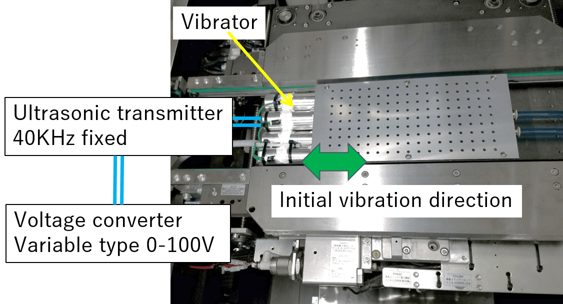
To apply vibrations, we manufactured a jig for attaching a vibrator to the PWB stage, as shown in Fig. 4, and evaluated the vibrations by switching the vibrator load voltage to 30 V and 100 V. In this evaluation, using a laser Doppler vibrometer, we measured the vertical vibrations in the PWB stage, the PWB of interest, and the stencil.
Then, to determine the relationship between vibration amount and printability, the same evaluation as in Section 3.2 was performed without vibrations applied (hereafter “0 V load voltage”) and then with the load voltage set to 30 V and 100 V. The vibration was continuously applied from when the squeegee descended and came into contact with the stencil until the stencil separation completed. Moreover, the two stencil surface coatings, one hydrophilic and the other water-repellent, underwent evaluation at the 100 V load voltage to examine their influences.
| ✓···Item of measurement/evaluation interest | Load voltage V | |||
|---|---|---|---|---|
| 0 | 30 | 100 | ||
| Vibration measurement | Laser Doppler vibrometer | ✓ | ✓ | |
| Print evaluation | Solder: A Stencil: no coating |
✓ | ✓ | ✓ |
| Solder: A Stencil: hydrophilic coating |
✓ | |||
| Solder: A Stencil: water-repellent coating |
✓ | |||
4.2 Evaluation results
During vibration measurement, vibrations were detected in the PWB stage, the PWB of interest, and the stencil. Table 10 shows the results of vibration measurement at the PWB pattern for the aspect ratio of 2.7. The vibrations detected at the 100 V load voltage were greater in the order of the PWB of interest, the PWB stage, and then the stencil. The PWB of interest consisted of glass epoxy resin and the copper foil. The difference in natural frequency between these materials resulted in vibration amplification, which was probably the cause of why the PWB of interest showed the highest value. Additionally, at the 30 V load voltage, the PWB of interest and the PWB stage showed the same amount of vibration, while the stencil showed the smallest amount of vibration.
| Vibration amount | |||
|---|---|---|---|
| Load voltage 30 V | Load voltage 100 V | ||
| PWB stage | 0.06 μm | 0.10 μm | |
| PWB of interest | 0.06 μm | 0.20 μm | |
| Stencil | 0.03 μm | 0.06 μm | |
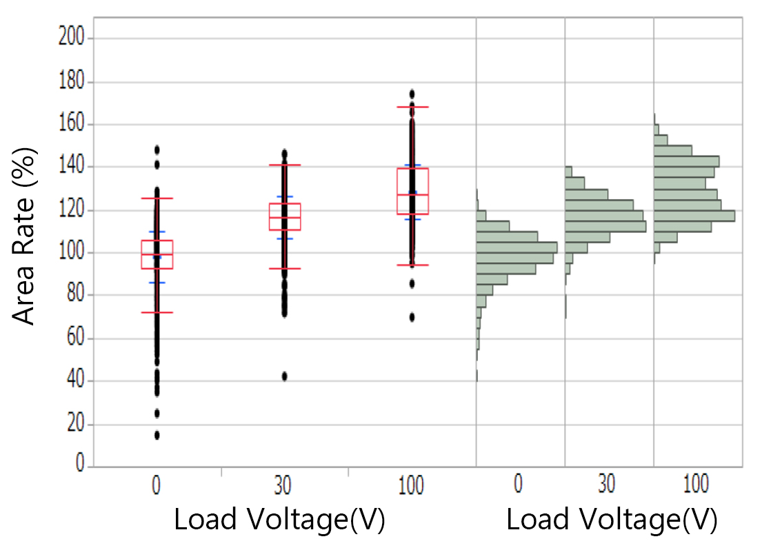
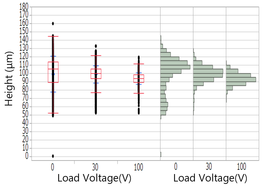
Next, we evaluated printability while changing the vibration amount by load voltage switching. Figs. 5 and 6 show the changes in the average area ratio and average height, respectively, as the print results for the aspect ratio of 2.7. Because the area ratio increased and the height decreased with the increase in load voltage, the wetting and spreading of the solder is considered to have increased as the vibration amount increased. Besides, as shown in Fig. 7, printing at the 100 V load voltage led to fewer stencil apertures clogged with solder, suggesting an increase in the area with good contact between the solder and the PWB pattern.
| Load voltage | Average (%) | Standard deviation (%) |
|---|---|---|
| 0 V | 97.8 | 12.0 |
| 30 V | 116.4 | 9.8 |
| 100 V | 128.3 | 12.9 |
| Load voltage | Average (μm) | Standard deviation (μm) |
|---|---|---|
| 0 V | 99.1 | 21.7 |
| 30 V | 98.7 | 10.1 |
| 100 V | 93.5 | 6.9 |
| After use stencil opening | |
|---|---|
| Load Voltage 0V | Load Voltage 100V |
 |
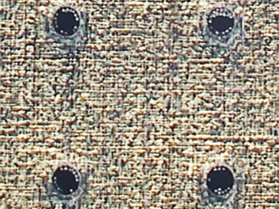 |
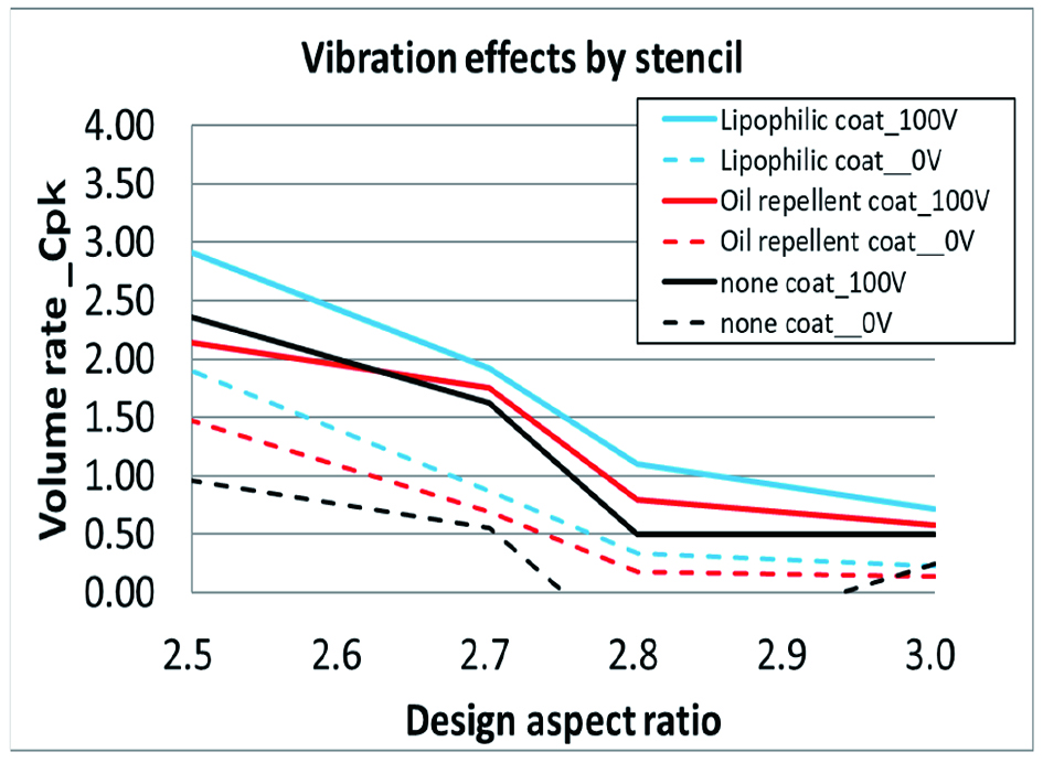
Fig. 8 shows the print results by the type of stencil surface coating. Regardless of the surface coating type, the Cpk value at the 100 V load voltage improved by approximately 1.0 from that at the 0 V load voltage. Hence, the difference in the coating type made no difference to the vibration effect. A Cpk value of 1.92 was achieved at the aspect ratio of 2.7 as the result of vibration application under conditions consisting of an optimally selected combination of solder properties, stencil surface coating, and PWB design.
| Design aspect ratio | ||||||
|---|---|---|---|---|---|---|
| Solder | Stencil | Load voltage | 3.0 | 2.8 | 2.7 | 2.5 |
| A | Hydrophilic coating | 0 V | 0.23 | 0.34 | 0.87 | 1.90 |
| 100 V | 0.72 | 1.10 | 1.92 | 2.91 | ||
| A | Water-repellent coating | 0 V | 0.14 | 0.18 | 0.69 | 1.47 |
| 100 V | 0.58 | 0.80 | 1.75 | 2.13 | ||
| A | No coating | 0 V | 0.25 | 0.00 | 0.56 | 0.96 |
| 100 V | 0.49 | 0.50 | 1.62 | 2.35 | ||
4.3 Summary of the vibration effect
To obtain the thrust force for bringing the solder required for printing at the aspect ratio of 2.7 into good contact with the PWB pattern, we evaluated the effect of solder fluidity improvement by ultrasonic vibration. After the vibrations, the PWB stage, the PWB of interest, and the stencil showed an increase in print area ratio and a decrease in print height. Meanwhile, fewer stencil apertures became clogged with solder. These results suggest that the application of vibrations leads to increased solder fluidity and yields the effect of improved printability.
5. Conclusions
Where mixed mounting is needed for components of various sizes from 0402 to large, it is required to perform printing with the solder filling rate stabilized for Size-0402 components at an aspect ratio that does not reduce the bonding strength of large components.
This time, we sought to achieve the target Cpk value of 1.8 while increasing the aspect ratio to 2.7 from 2.4 last time. We found that the key to successful high aspect ratio printing was to increase the adhesion force between the solder and the PWB pattern by bringing them into good contact with each other. Therefore, proper selection must be made of a combination of solder properties, stencil surface coating, and PWB pattern design as the set of conditions that facilitate the flow of solder into stencil apertures. Even with the optimally selected combination of conditions, however, the highest Cpk value achievable at the aspect ratio of 2.7 was limited to 0.87. Then, we resorted to vibrational energy application to increase the thrust force for bringing the solder into contact with the PWB pattern and obtained an improved Cpk value of 1.92. We concluded that vibration printing thus provided an effective method of high aspect ratio printing.
We have just begun basic data collection and printability evaluations for the technical evaluation of vibration printing. This technology needs further evaluations regarding many factors involved, such as the repeatability of vibrations, the stability of the PWB surface, the effect of patterns other than resist opening patterns, and the influences on mounted components. We intend to perform further evaluations toward the practical application of this technology to FA equipment for stable mass-production of printed wiring boards mounted with a mix of Size-0402 and larger components.
References
- 1)
- Y. Koji, “High Aspect Ratio Solder Printing Technology Enabling Mixed Mounting From 0402 Components to Large Components,” (in Japanese), OMRON TECHNICS, vol. 51, no. 1, pp. 149 – 154, 2019.
- 2)
- Jisso Technology Roadmap Group, “Chapter 4, Electronic Components,” in JEITA Jisso Technology Roadmap 2017, Japan Electronics and Information Technology Industries Association(in Japanese), 2017, p. 257.
- 3)
- K. Yuichi, H. Akihiko, and Y. Mobuhiro, “Printed Wiring Board Technologies for Thin and Light PCs” (in Japanese), Toshiba Review, vol. 60, no. 8, pp. 17-18, 2005.
- 4)
- Namics Co., Ltd., “Screen Printing Method and Apparatus of the Same,” Japanese Unexamined Patent Application Publication. No. 2010-149301 (P2010-149301A), 2010-7-8.
The names of products in the text may be trademarks of each company.