


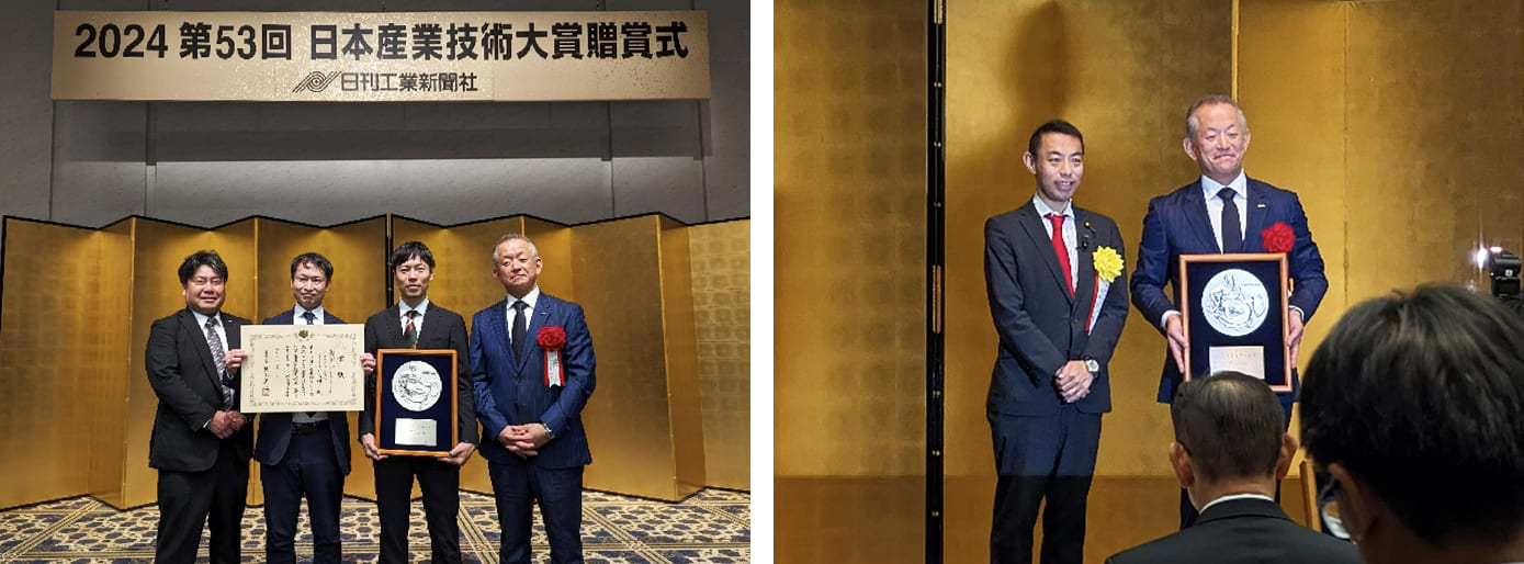
OMRON felicitated with the Minister of Education, Culture, Sports, Science and Technology Award at the 53rd Japan Industrial Technology Awards The High-Definition, High Speed In-Line CT-Type Automated X-Ray Inspection Technology pegged as an important innovation for the semiconductor industry
- April 08, 2024
OMRON Corporation (HQ: Shimogyo-ku, Kyoto; President and CEO: Junta Tsujinaga) announced today that it’s inspection technology for semiconductor chiplets, which was realized with the VT-X950 automatic CT-type X-ray inspection system announced in November 2023, has been awarded the Minister of Education, Culture, Sports, Science and Technology Award at the 53rd Japan Industrial Technology Awards (sponsored by Nikkan Kogyo Shimbun).
By combining OMRON's proprietary control and image processing technologies, the VT-X950 enables high-speed, high-precision inspection of advanced semiconductor packages. By combining the continuous imaging technology*1 and the high sensitivity camera by seamless control of the control equipment constituting the device, the 3D image is generated with high resolution and easy to distinguish. With the high resolution of imaging at 0.2 Ојm, it is possible to visualize the solder quality of ОјBump*2 and C4Bump*3 used in the 3D mounting of each semiconductor package. In addition, the high-speed generation of modeling utilizing the most advanced 3D inspection technology used in medical CT scanning enables in-line quality inspection, which was difficult at the manufacturing site. By utilizing our proprietary AI technology, we automatically optimize the setting of imaging conditions for inspection and automate the creation of inspection programs, which was difficult until now for experienced technicians.
The comments of the judging panel of the Japan Industrial Technology Award are as follows:
- It is a technology necessary for the advancement of the semiconductor industry and an important automated inspection technology for the improvement of semiconductor performance.
- It is possible to perform in-line inspection at 100 times higher speed than a typical analyzer.
- The minimum resolution per pixel for CT type X-ray inspection has been improved from 0.3 Ојm to 0.2 Ојm.
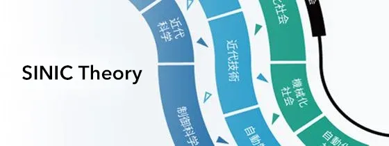
As further advances in semiconductor miniaturization and performance are expected, advanced inspection technology is essential for stable production and high quality. In addition to improving productivity at manufacturing sites, OMRON enrich the future for people, industries and the globe by innovative automation.
For more information, click here. Sorry for Japanese only.
Automatic CT X-Ray Inspection System "VT-X 950"
*1: Technology for imaging stereoscopic images without stopping while moving
*2: Bump electrode formed at a narrow pitch for bonding IC devices together
*3: Controlled Collapsed Chip Connection (C4) A bump shaped conductor protrusion is formed on the substrate electrode and bonded to the wafer
About the Japan Technology Award
The Japan Industrial Technology Award was established in 1972. Each year, the award system honors companies and groups that have achieved outstanding results in the development and practical application of innovative large-scale industrial equipment and structures, advanced technologies, and other advanced technologies. The purpose of the award is to recognize achievements that have contributed to the development of industry and society, and to encourage technological development.
![]()
Adobe Acrobat Reader is free software that lets you view and print Adobe Portable Document Format (PDF) files.