


High-speed Inspection Technology by Continuous Movement between Fields of View of Automated CT-type X-ray Inspection System
- CT
- X-ray
- Automatic inspection system
- Inline
- Solder inspection
In order to inspect the solder joints of invisible components on increasingly sophisticated automotive electronic circuit boards, we have been providing automated X-ray inspection systems using the CT method. However, our conventional technology, VT-X750-V1/V2 with continuous image capture control, repeatedly stopped and moved the image capture system stage when moving it to the field of view to be inspected, resulting in a loss of acceleration and braking time. To solve this problem, we developed a technology to eliminate this loss by performing acceleration and braking during the movement between fields of view and not stopping at the connection between the movement between fields of view and continuous image capture. As a result, the series of inspection movements can now be performed in a single stroke motion like “Spur” of the snowfield, thus realizing faster CT inspections. With this technology, the new VT-X750-V3 achieves an inspection speed 1.5 times faster than the previous model, enabling high-speed inspection that keeps pace with the evolution of customer boards. This paper introduces the latest technology in OMRON’s X-ray automated inspection systems that has greatly contributed to the higher speed.
1. Introduction
With a growing awareness of the Sustainable Development Goals (SDGs) aiming to build a sustainable society, zero emission efforts are being intensified worldwide. Consequently, there is a pressing need for activities to reduce CO2 emissions to prevent global warming. This urgency has further increased expectations for the broader adoption of electric vehicles (EVs).
This social trend is driving the automotive industry to pursue higher-density mounting of electronic control units (ECUs) and other electronic printed circuit boards (PCBs). The objective is to balance cabin space comfort and functional expansions. According to the Japan Jisso Technology Roadmap1), there is an increasing ratio of size 0402 devices (smaller than size 0603) among chip components mounted on electronic PCBs. The automotive industry, in particular, has stringent manufacturing quality requirements. Quality inspections are implemented to ensure a safe and secure society that is free from traffic accidents. For instance, in vehicle-borne component factories in Europe and North America, the prevailing method of inspection for electronic PCBs is not sampling inspections but rather 100-percent inspections. This approach requires measuring solder shapes to inspect joints for strength.
Responding to such social trends, OMRON has spread the use of automated X-ray inspection (AXI) systems as equipment that can inspect soldered parts on the visually inaccessible underside of components in surface mount technology (SMT) production lines. This paper presents our VT-X750-V3 technology (Fig. 1), which has eliminated inspection time losses due to inter-FOV movement, a challenge in the previous technology, achieving further speed improvements.

2. CT method-based AXI for achieving high image quality
2.1 Solder defect modes in visually inaccessible places
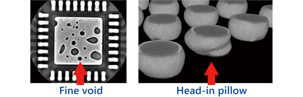
The technical background factors behind the recent remarkable trends toward smaller, lighter-weight, and higher-performance electronic equipment are higher-density integration of components, finer patterns of PCBs, and multilayer mounting. Situations are increasing where solder joint inspection is difficult with automated optical inspection (AOI) and other visual inspection methods. For example, defect modes encountered in ball grid array (BGA) inspections include fine voids (cavities) sized on the order of several tens to hundreds of μm or unwetting and other forms of unmelted solder (Fig. 2). More than 1,000 solder joints in each BGA package must be inspected to ensure the electrical safety and reliability of such electronic equipment.
2.2 Comparison of X-ray image diagnosis methods
Image diagnosis methods using X-rays broadly fall into the transmission and CT methods (Fig. 3).
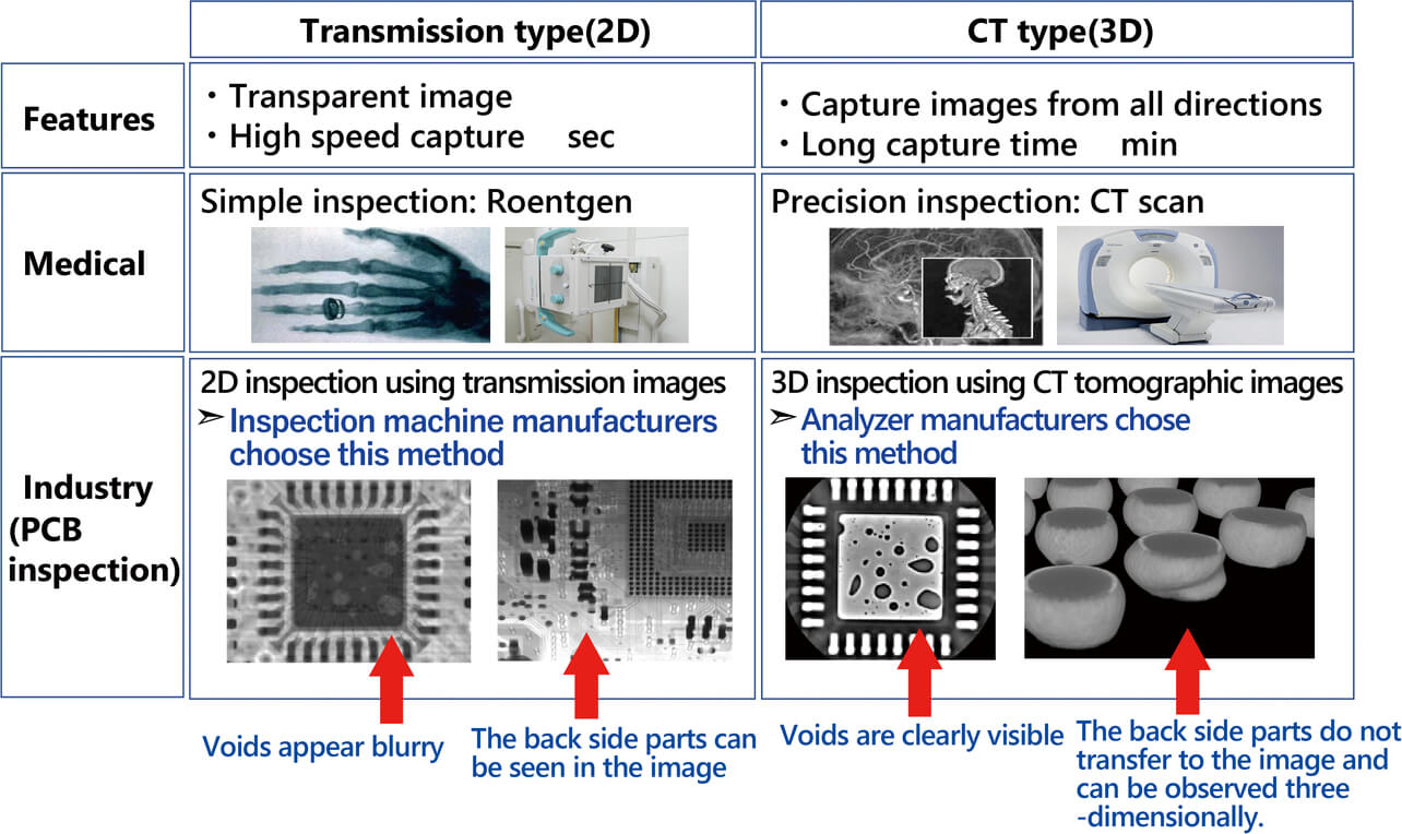
The transmission method utilizes two-dimensional (2D) images, similar to radiographic medical photography. Because of its inherent characteristics, this method faces challenges in obtaining fine images of inspection points and often ends up with images where the target object overlaps with show-through underside-mounted components. However, the 2D method provides higher inspection speeds and smaller data sizes, thus becoming a preferred choice for manufacturers of PCB inspection machines that require high-speed inspection capabilities.
On the other hand, the CT method captures and obtains images from all around 360 degrees using an X-ray camera or a similar device and then reconstructs them into three-dimensional (3D) data. What characterizes this method is its ability to generate clear reconstructed 3D images, which are fine stereoscopic images free from overlaps with show-through underside-mounted components. However, this method handles larger-sized data and captures images from all around 360 degrees, resulting in a slower and more time-consuming inspection process than with the transmission method. As a result, this method is primarily adopted by manufacturers of analysis equipment for applications involving detailed analysis of faulty products.
2.3 OMRON’s AXI
We consider it one of our missions to provide high-precision, high-speed PCB inspection machines that ensure the high quality of electronic PCBs, making our society safer and more secure. The transmission method often produces images with blurry voids or show-through components mounted on the underside of PCBs, making it unsuitable for precisely inspecting fine voids or unmelted solder balls. Therefore, we have focused on providing CT method-based AXI solutions. In 2009, we released the VT-X700, followed by the VT-X750-V1 in 2017, which boasted an inspection speed twice as fast as the X700, and the VT-X750-V2 in 2018, which featured even higher resolution. We have successfully addressed a variety of customer needs, including BGA void inspections, Solder fill rate in through-holes inspections for inserted components, and more2).
Now, let us present here the component technologies of our AXI system. Our AXI system comprises a combination of different technological elements, enabling high-precision inspections based on many insights accumulated through our experience with AOI. The key technological elements here include an imaging device for high-resolution image generation, high-precision geometry design and control, robust image correction capabilities, and an algorithm for that purpose.
2.4 High-definition image generation devices (FPD and X-ray source)
A flat panel detector (FPD) is a camera that converts X-rays into light through a fluorescent substance called a scintillator and then into electrical signals to obtain digital images. The FPD captures luminance information pixel by pixel and can produce high-definition and high-sensitivity images.
X-ray sources broadly divide into two types: open and closed tubes. Closed tubes feature a filament and a target, which have a longer life span compared with open tubes, making them more suitable for long-time in-line inspection at a lower running cost. Our AXI system adopts a lightweight micro-focus closed tube source that provides a necessary and sufficient dose and a focus diameter on the order of micrometers (μm).
2.5 High-precision geometry design and control
2.5.1 Geometry configuration
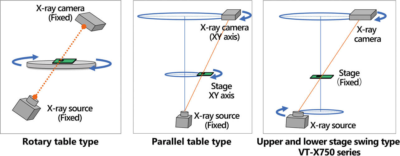
For the geometry design of our AXI system, we have adopted the parallel-table type instead of the rotary-table type. This type obtains CT images using orthogonal movements in the XY-axis direction to change the relative position of the X-ray source or the FPD to the target object. We adopted this type because the rotary-table type produces a round and narrow field of view of 3D data, easily resulting in blurs along the edges of images. Additionally, the limited rotational speed of the rotary-table type poses limitations on increasing the imaging speed3). While our older model (VT-X700) and our competitors’ models are of a type that involves turning the stage and the camera, the VT-X750 and subsequent series have a upper and lower stage swing configuration, eliminating the need to rotate the conveyor stage to avoid placing additional loads on the inspection target object (Fig. 4).
2.5.2 Continuous imaging technology
This sub-subsection describes the continuous imaging control technology integrated into the VT-X750 and subsequent series. This technology has the following two key features:
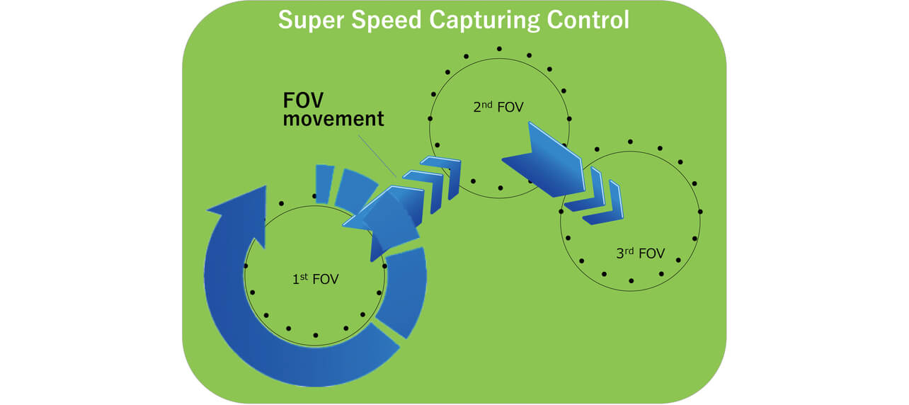
The first feature involves the continuous movement of the X-ray camera and the source stage during a turn-and-capture operation. This technology aims to obtain all the images corresponding to one field of view during an uninterrupted rotation, thereby reducing the imaging time per field of view (Fig. 5).
The X-ray camera and the source stage repeat a turning action at a constant speed. Therefore, ensuring the synchronous operation of their respective axial motors is crucial for achieving high-precision turning paths. This technology is built upon OMRON’s products, specifically the NJ and NX Series programmable logic controllers (PLCs) and 1S Series servomotors and drivers. The multi-axis synchronous control technology based on these devices, in conjunction with high-rigidity hardware, has made high-precision continuous imaging technology a reality.
The second feature is a high-speed imaging and data processing system with enhanced speed. A system capable of rapid imaging, even with the mechanism in operation, has been developed as an imaging trigger system synchronized with axis actions. It has been known that images captured with the mechanism moving are prone to blurring4). To reduce blurs, the X750 Series incorporates a unique reconstruction technology (3D image generation process) and high-speed imaging exposure control. The image reconstruction and overall system processing speeds are optimized primarily using a graphics processing unit (GPU).
2.6 Robust correction processing and algorithm
Our AXI system relies on its hardware and dedicated application software to enable high-precision inspection of solder joint surfaces.
For example, when PCBs (workpieces) are introduced into the system for inspection, their stopping positions may vary. Therefore, the AXI system has a visible-wavelength LED light source and a small camera to correct such variations. By capturing images at visible wavelengths, our AXI system corrects feeding stop position variations or rotational deviations among workpieces on the conveyor. This approach capitalizes on the familiarity of human eyes with moving and still images captured at visible wavelengths, making it easier for the operator to verify the intended target component’s position during inspection program creation.
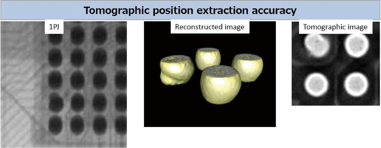
High-precision image processing requires high-precision extraction of correct tomographic positions after reconstruction. Our AXI system achieves this using OMRON-made displacement sensors and controllers provided on it. These devices measure the warpage and deflection amounts of workpieces and correct the height positions of the surfaces under inspection to generate high-precision images (Fig. 6).
3. Challenges to keeping pace with advancements in PCBs
When the matter comes to enabling in-line inspection while keeping pace with advancements in customers’ PCBs, the CT method encounters a significant challenge. The challenge lies in enabling inspections at higher speeds and with lower exposures, all while ensuring that high image quality is maintained.
3.1 Challenge to achieving further inspection speed improvements
The CT imaging method provides high-precision image quality but requires a longer inspection takt time (the time needed to inspect a single workpiece). This is because the CT method involves capturing images during a 360-degree rotation, as mentioned earlier. Because the AXI system is a post-process system in the PCB mounting line, it must meet the required in-line inspection takt time to maintain the line’s production efficiency. If the system fails to meet these requirements and compromise the line’s production efficiency, it will not be adopted by customers with demanding needs for an increasingly shorter inspection takt time or 100-percent inspection. The inspection speed achievable by the AXI system affects customers’ PCB production efficiency, resulting in the recent increasing demand for faster inspection speeds. For instance, an inspection speed of approximately 30 seconds or less per M-size PCB (around 200 mm × 200 mm) has become more commonly requested. One technical issue particularly relevant to continuous imaging is the time lost during acceleration and deceleration for turn-and-capture operations which occur when stops are made during inter-FOV movement. Taking note of these time losses, we decided to eliminate them to achieve further speed improvements.
3.2 Challenge of reducing exposures to workpieces under inspection
Another challenge lies in controlling the exposure to workpieces under inspection. PCBs are becoming increasingly dense with a growing number of exposure-vulnerable components, such as semiconductor devices or ICs. Consequently, it has become necessary to reduce the exposure level for workpieces under inspection while maintaining the level properly.
Our conventional VT-X750-V1 and V2 systems (hereinafter referred to as the V1 and V2 systems) included a function to predict and indicate the overall exposure to the entire PCB. However, this function could not calculate exposures for individual IC components. As a result, customers had to use the overall exposure to the entire PCB as an estimate for IC components, resulting in too high an exposure value for IC components. Thus, customers were forced to set X-ray irradiation doses to conservative levels. However, imaging with reduced X-ray doses leads to decreased image quality, making it impossible to perform inspection under optimal imaging conditions. Conversely, in some cases, certain components were exposed to excessively high X-ray doses, leading to increased exposures.
Therefore, the challenge lies in enabling customers to properly control exposures on a component-by-component basis to reduce exposures to workpieces during inspections.
4. VT-X750-V3 for achieving further inspection speed improvements
We have developed a technology that solves the challenges discussed in Section 3. This section first describes the inter-FOV continuous movement technology, which has been integrated with our conventional continuous imaging technology to achieve further speed improvements. Then, this section presents exposure heatmaps obtained by applying the control parameters of the inter-FOV continuous movement technology.
4.1 Inter-FOV continuous movement
This section provides a detailed explanation of the newly developed inter-FOV continuous movement technology. This subsection defines the following terms to help better understand this technology:
- (i)
- Field of view and (ii) inter-FOV movement.
- (i)
- Field of view (FOV)
This term refers to an imaging area used to generate a reconstructed stereoscopic image at an inspection point. From a control perspective, a field of view represents the turning path area drawn by the imaging device in the top-view perspective for looking into the system from its top face.
- (ii)
- Inter-FOV movement
This term denotes the movement between two inspection points. From a control perspective, an inter-FOV movement represents a path followed by an imaging device in the top-view perspective, as with a FOV, from one clearance circle to another.
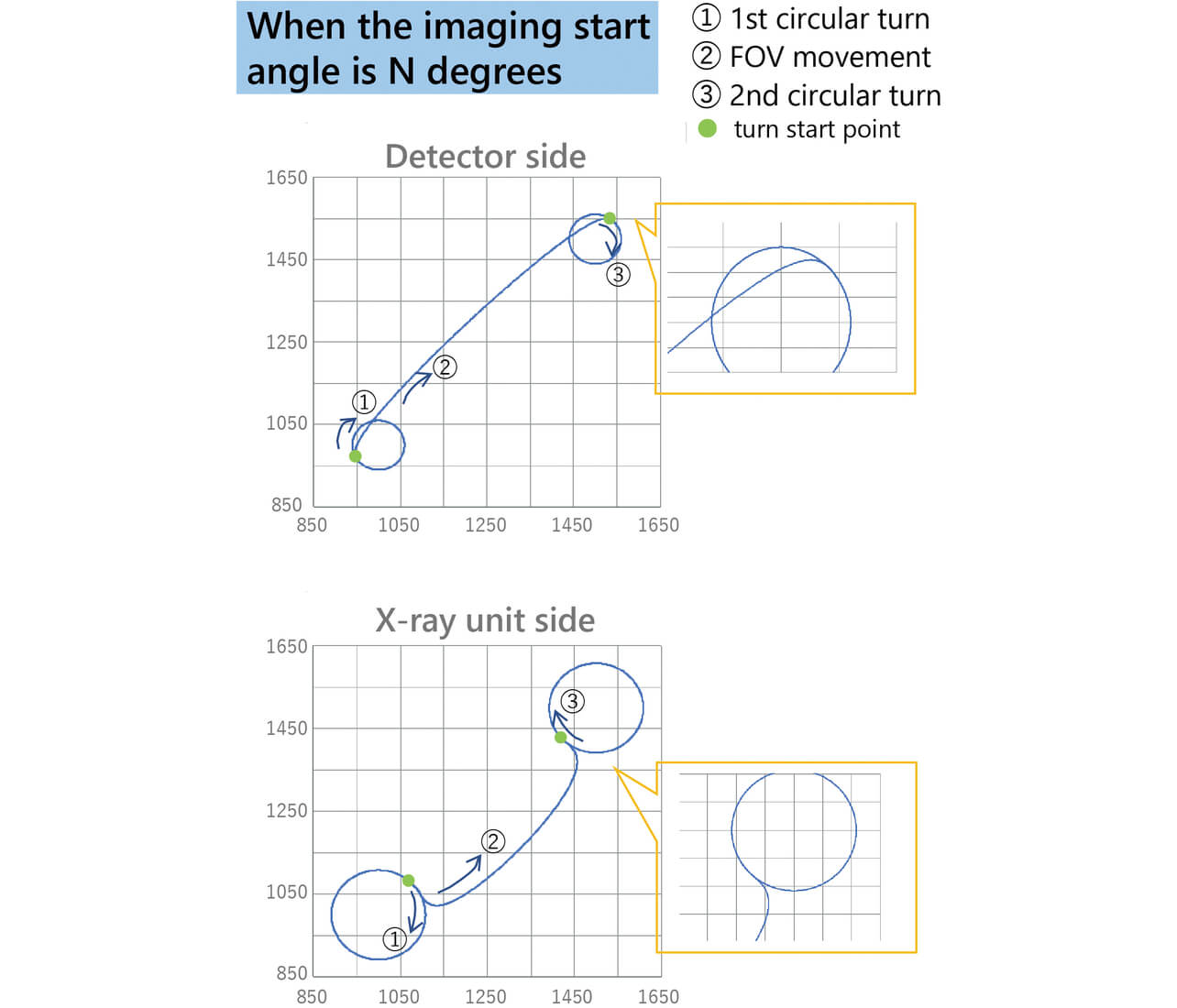
Fig. 7 illustrates these two concepts:
4.1.1 Method of implementation and features
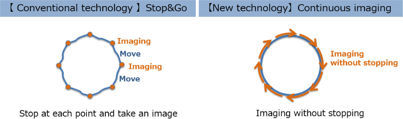
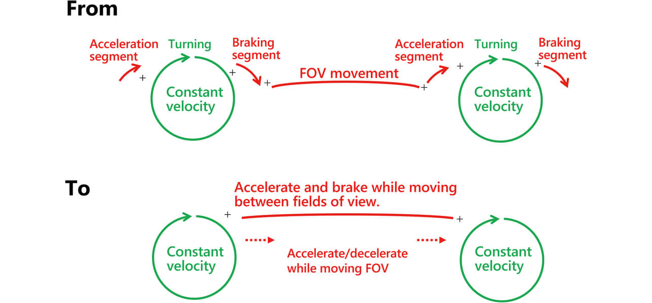
Continuous imaging requires a constant-speed turning action to obtain high-precision images. In the older systems up to V1 and V2, a stop was made for each FOV rotation, necessitating an acceleration segment for turning at a constant speed and a braking segment for braking. These acceleration and braking processes take time. To solve this problem by making these processes occur during inter-FOV movement, we developed the inter-FOV continuous movement technology. This technology aims to eliminate the time taken for acceleration/braking during each FOV rotation, enabling a seamless, stop-free operation even during transitions between inter-FOV movement and imaging (Fig. 8).
This technology was developed as an OMRON-proprietary technology*1 and implemented through seamless synchronous control of OMRON-made PLCs, multi-axis servomotors, and control software. This inter-FOV continuous movement technology offers the following four features:
1. Inter-FOV movement free of braking segments
As mentioned earlier, the most important feature is that the acceleration necessary for the next clearance circle occurs, but without any braking segment, during the current inter-FOV movement. This feature enables a series of inspections to be performed without any interruptions.
2. Controllable not to exceed the device’s maximum allowable acceleration
The parameters related to the speed during inter-FOV movement can be continuously controlled. In addition, the next FOV rotation can also start from zero acceleration at the starting point. This feature allows for movements without any loads applied to the imaging device.
3. Selecting a travel route for the least time-consuming movement
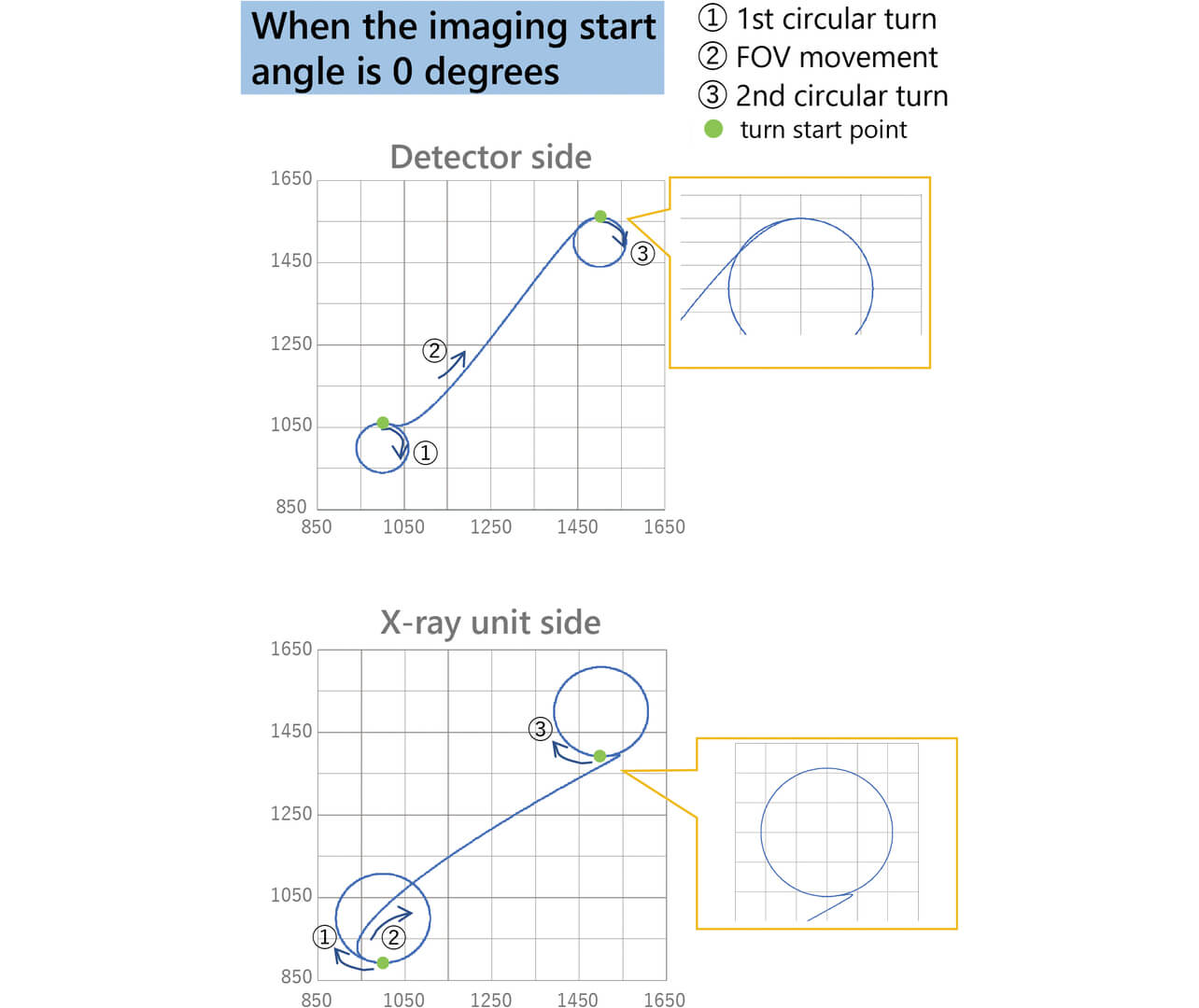
Imaging can be initiated even with an incident angle other than 0° over the starting point of the next clearance circle (Figs. 9 and 10). A travel path is derived that does not exceed the device’s maximum allowable acceleration and allows for the least time-consuming movement based on the calculation results for speed-related control parameters. This approach reduces the time required to move to the next clearance circle.
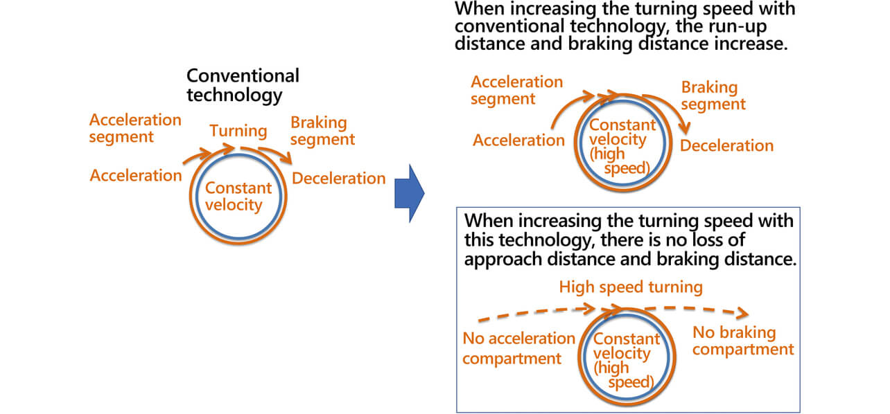
4. Enabling further turning speed improvements
Attempting to increase the turning speed with the previous technology would pose a problem. The issue arises from the fact that turning control requires a turning action at a constant speed to ensure high-precision image quality, which is why a run-up distance and a braking distance were provided. As a result, a turning action at a constant but increased turning speed would require extending the acceleration and braking distances. However, the new technology provides a solution to this problem. With this technology, acceleration and braking actions occur during inter-FOV movement, eliminating the need for large run-up or braking distances even at faster turning speeds (Fig. 11).
4.1.2 Effects of the inter-FOV continuous movement technology
This sub-subsection presents the speed-up effects achievable with the inter-FOV continuous movement technology through a comparison with the previous technology for theoretical and measured values.
The measured values available were the acceleration and braking segments’ time equivalents included in the turning time. Hence, the two technologies were compared for the turning time.
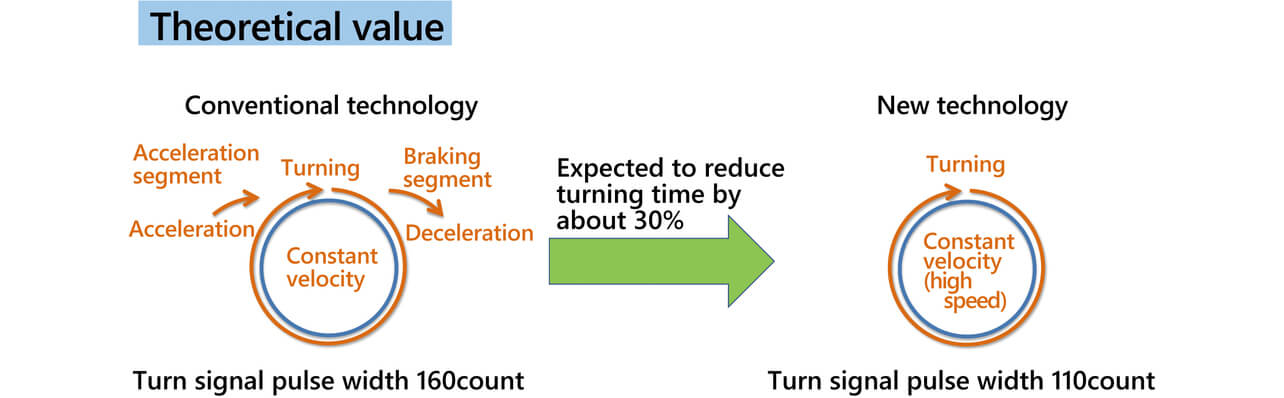
A PLC-based data trace method was employed as a check method. Turning signal pulse widths (counts) per FOV rotation were obtained for comparison. The two technologies were compared regarding the second FOV’s turning time during three FOV rotations and two inter-FOV movements to evaluate the decreases in acceleration and braking segments. The previous technology would have a theoretical pulse width of 160 (counts) per turning time. Meanwhile, the new technology would have a theoretical value of 110 (counts) per FOV, considering the absence of acceleration and braking times. As a result, the latter technology would reduce the turning time by approximately 30 percent compared with the former (Fig. 12).
Now, let us examine the measured results. The previous technology and the new technology yielded measured values of 155 (counts) and 109 (counts), respectively (Fig. 13 and Table 1). The difference between the theoretical and measured values for the previous technology can be attributed to the axis settling time, which was six counts long. Consequently, the measured value obtained aligned well with the theoretical value. Thus, the turning time was reduced by approximately 30 percent, indicating the successful elimination of the acceleration and braking times.
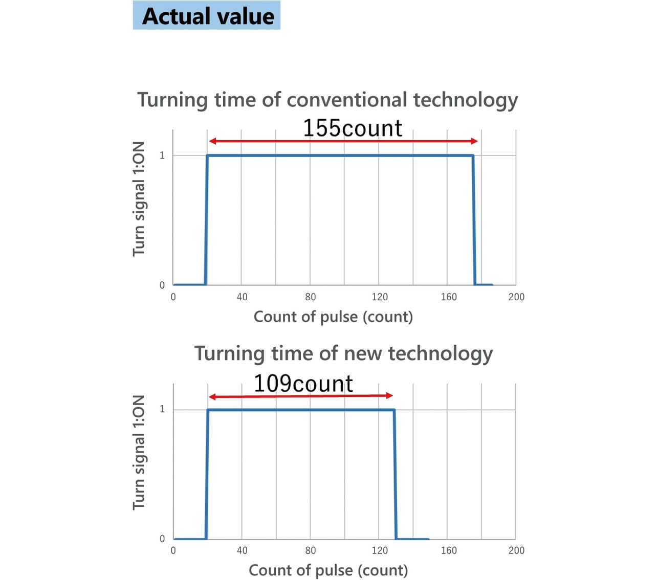
| FROM previous technology Turning signal pulse width [counts] | TO new technology Turning signal pulse width [counts] |
|
|---|---|---|
| Theoretical value | 160 | 110 |
| Measured value | 155 | 109 |
4.2 Effects of speeding up the inspection time
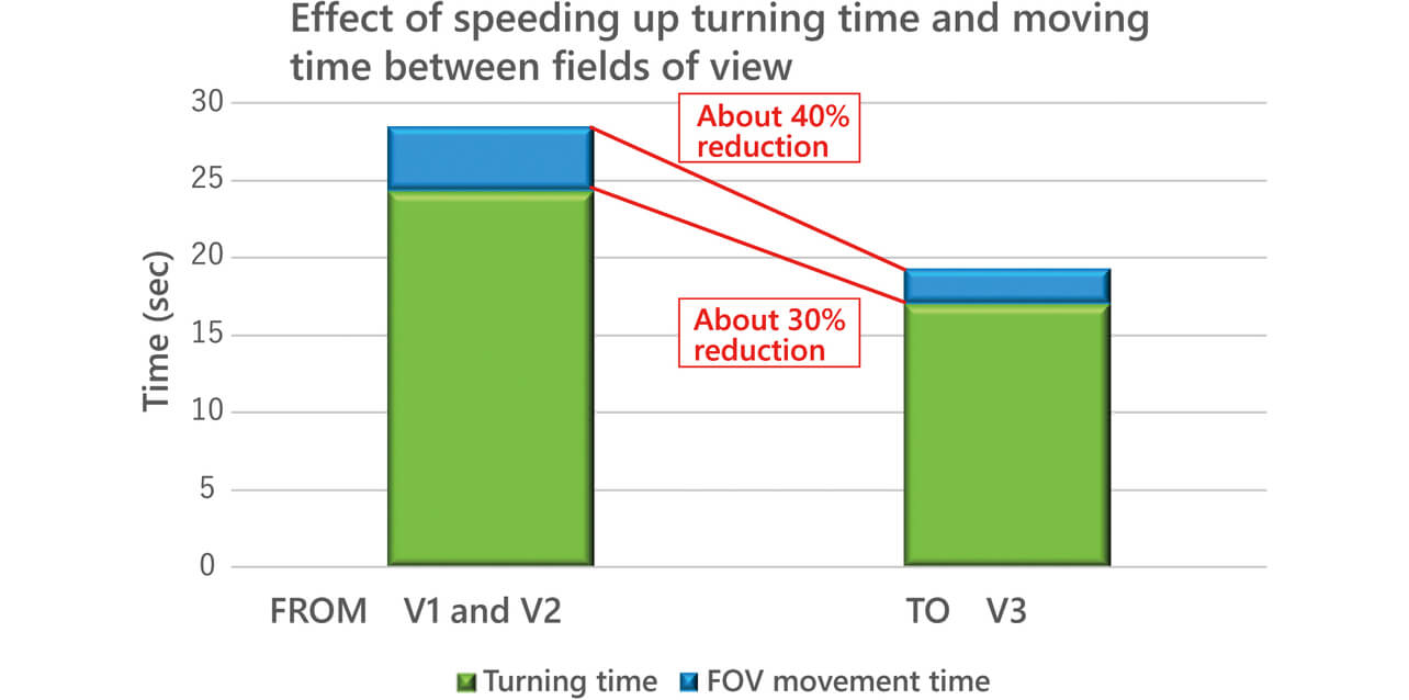
This subsection presents the actual effects of PCB inspection time reduction achieved through the combination of continuous imaging and inter-FOV continuous movement. The previous and new technologies were compared for the sum of the turning time and inter-FOV movement time, using eight FOVs’ worth of images captured from a customer’s PCB. Data collection was conducted using the V2 and V3 systems. The log outputs from each system were aggregated for estimation. The results revealed a reduction of approximately 40 percent in inter-FOV movement time and 30 percent in turning time (Fig. 14)*2. From these observations, the new technology significantly contributed to achieving an inspection speed 1.5 times faster than before.
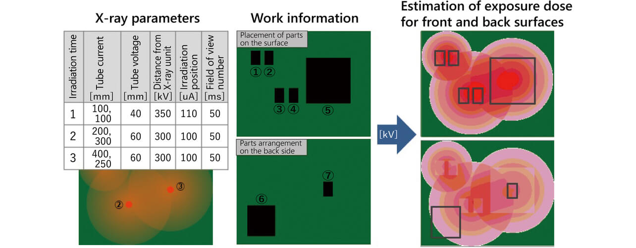
4.3 Enabling low-exposure CT inspections
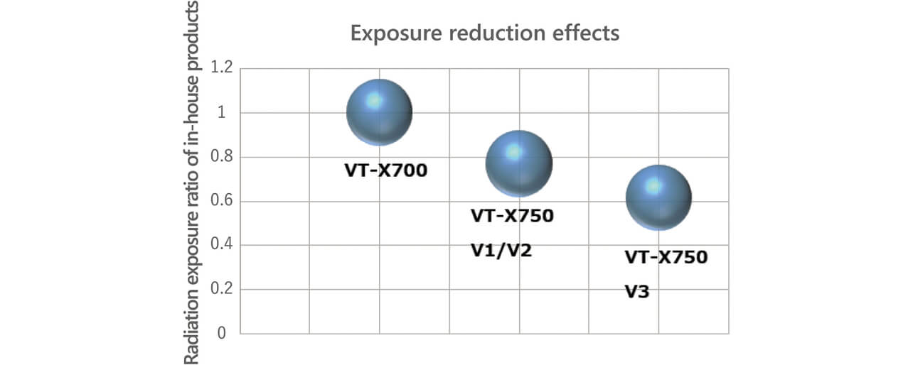
This subsection highlights additional benefits of the inter-FOV continuous movement technology. By applying the parameters for computing paths during inter-FOV movement, this new technology enables the prediction and representation of component-by-component exposures in heatmap format (Fig. 15)*3. This heatmap capability has enabled customers and front-end engineers to create inspection programs with optimized irradiation conditions for components. As a result of exposure reduction effects through speed enhancement and irradiation condition optimization through heatmaps, the V3 system based on this new technology achieved a further approximately 20 percent reduction in exposure compared to the V1 and V2 systems and a 40 percent reduction5) relative to the X700 system*2. These findings demonstrate that the advancements in our inspection technologies have led to faster inspection speeds and lower exposures to workpieces (Fig. 16).
5. Conclusions
To address the challenge of reducing losses during inter-FOV movement in our conventional continuous imaging technology, we developed the inter-FOV continuous movement technology. Despite still using the CT method, this technology further improved inspection speed. With this technology, the VT-X750-V3 system can now inspect a broader range of customers’ products, including electronic PCBs. Taking advantage of the opportunity offered by this paper, the author would like to express his sincere gratitude to our development team and the Motion Control Division’s development team for their dedicated efforts in bringing this new technology to fruition.
Moving forward, we intend to keep pace with advancements in customers’ PCBs and products while addressing further improvements in inspection speed. We believe that our inspection technology can be applied to diverse electrical equipment parts and components, extending beyond the electric vehicle industry. For instance, in the energy infrastructure industry, including the renewable energy sector, batteries designed to mitigate weather-induced variations in renewable energy power outputs will become widespread, along with broader deployment of transmission efficiency-improving equipment, including long-distance transmission efficiency-enhancing equipment, such as high-voltage DC transmission cables and superconducting cables. Additionally, with fifth-generation (5G) mobile communication systems, the information and communication infrastructure industry are preparing for base station deployment and frequency allocation to enable high-capacity, low-delay, and multiconnection communication services. PCBs and components used in such facilities include devices equipped with thick heat sinks, insulated gate bipolar transistors (IGBTs), field effect transistors (FETs), and other power module products utilizing wide-gap semiconductors, such as silicon carbide (SiC) or gallium nitride (GaN), as well as large PCBs designed for 5G base stations. To ensure effective detection of soldering defects in these products, we intend to explore high-speed imaging technologies able to capture low-exposure, high-contrast images rapidly.
A new society is emerging where values and services that merge physical and cyberspaces are continuously being created. In an increasingly electrified society, we will continue to provide product inspections for various electrical parts and components to enhance customers’ product quality, thereby contributing to building a sustainable, safe, and secure society.
Notes:
- *1:
- Patent registered
- *2:
- By in-house comparison
- *3:
- Patent applied for
References
- 1)
- Jisso Technology Roadmap Committee, “2022 Edition of the Japan Jisso Technology Roadmap,” Japan Electronics and Information Technology Industries Association (in Japanese), 2022, p.352, 450-451.
- 2)
- M. Shichiro, “Development of Super High-Speed CT X-Ray Automatic Inspection System,” (in Japanese), OMRON TECHNICS, vol. 51, no. 1, pp. 91-97, 2019.
- 3)
- S. Sugita, “High-Speed CT Inspection Technology for Wider Coverage of Mounting Quality Assurance,” (in Japanese), in Proc. 52nd Soldering Breakout Session, Japan Welding Society, 2011, p. 4.
- 4)
- Japanese Society of Radiological Technology, Supervising Ed., K. Ichikawa and Y. Muramatsu, Eds., “Standard X-Ray CT Image Measurement,” Ohmsha, (in Japanese), 2009, pp. 27-28.
- 5)
- T. Onishi, “In-line Automated X-Ray Inspection System with High-Speed, High-Resolution, Low-Dose Inspection Capability,” (in Japanese), Image Laboratory, vol. 29, no. 1, pp. 67-72, 2018.
The names of products in the text may be trademarks of each company.