Corporate | Global
We are Shaping the Future!Showcasing Success Stories as We Innovate for a Sustainable Tomorrow
Integrated Report 2024: Long Term Vision SF2030 Topics
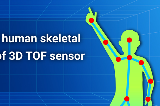
Under SF2030, OMRON aims to contribute to "realization of a digital society," where people are free from restrictions and can pursue individual fulfillment.
For example, this will be a society where the evolution of automation combined with control devices supports the spread of advanced technology, allowing everyone to be creative in their own way. Generative AI and high-speed communication technologies such as 5G/6G are shaping the digital society of the near future, as are smartphones and IoT devices that are now integral to our lives. Semiconductors are incorporated in these products and technologies, underpinning technological innovation. The strategic importance of semiconductors has gained widespread recognition. Semiconductors, which are at the heart of myriad products, are always subject to quality issues.
Semiconductor chips have traditionally achieved higher performance through miniaturization of the wiring width of device and circuits, but the technical challenge of microfabrication technology has increased with the passage of time, making it increasingly difficult to produce non-defective products. In the case of advanced semiconductors, the costs of R&D and production equipment have soared, pushing manufacturing costs ever higher. Therefore, improvement of pass yields has become a crucial challenge. To address such technological issue, a new technology, the "chiplet" (see Fig. 1), which involves fitting multiple tiny semiconductor chips into a single package, is attracting attention as a means of improving performance in addition to miniaturization. On the other hand, in contrast to conventional planar designs (monolithic), 3D mounting makes chiplets' structures more complex. This means that transmission images obtained by 2D X-ray inspection systems are of limited effectiveness as a basis for determining whether chiplets are non-defective. A means of inspection offering greater precision is required. The VT-X950 high-speed in-line CT-type X-ray automatic inspection system unveiled in November 2023 enables high-speed, high-precision inspection. (See Fig. 2)
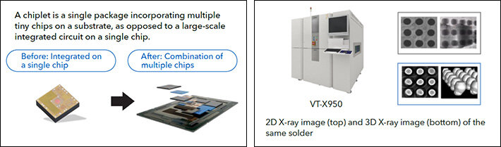 Fig. 1 Semiconductor Industry's Evolution and Challenges / Fig. 2 VT-X950 CT-type Automatic X-ray Inspection System and X-ray Images
By combining OMRON's proprietary control and image processing technologies, VT-X950 achieves high-speed, high-precision inspection of advanced semiconductor packages. Utilizing state-of-the-art 3D CT technology, the system captures images with resolution as small as 0.2 μm (1 μm is 1/1000 of 1mm), visualizes the quality of minute amounts of solder inside semiconductor packages, and enables automatic judge of good/defective by means of quantitative inspection. Through utilization tailored to customers' specific applications, the VT-X950 will contribute to higher development speed, yield improvement, and stabilization of mass-production quality in all phases of semiconductor manufacturing, from R&D through to mass production. (See Fig. 3)
The VT-X950's high-definition, high-speed in-line CT-type automated X-ray inspection technology for semiconductor chiplets received the Minister of Education, Culture, Sports, Science and Technology Award at the 53rd Japan Industrial Technology Awards. Comments of the panel of judges included the following: "It is a technology necessary for the advancement of the semiconductor industry and an important automated inspection technology for the improvement of semiconductor performance," and "The minimum resolution per pixel for CT type X-ray inspection has been improved from 0.3 μm to 0.2 μm."
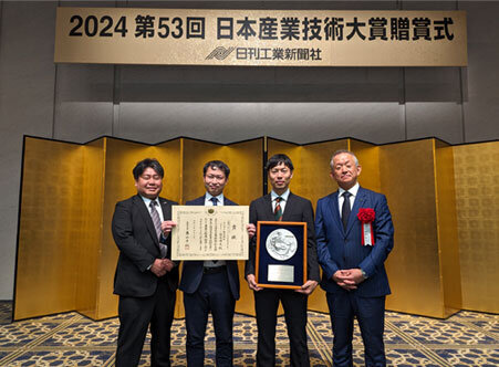 Received the Minister of Education, Culture, Sports, Science and Technology Award at the Japan Industrial Technology Awards
(Far right) Kazuhisa Shibuya, Senior General Manager, Inspection Systems Business Division HQ,
Industrial Automation Company, OMRON Corporation
In addition to the model for advanced semiconductors, OMRON developed the VT-X850, a model for power semiconductor modules, to meet the inspection needs of the automotive industry. With their excellent environmental credentials, EVs will be a primary means of transportation in the emerging digital society. Integration (X in 1) of components that combine multiple functions, such as the "eAxle," which is an integrated unit comprising major power devices such as gears, motors, and inverters in EVs, has become the technological mainstream. As more items must be inspected because of the increasing complexity of the internal structure, the need for high-resolution 3D inspection is increasing. The VT-X850 uses a high-power X-ray tube suitable for large, thick power semiconductor modules, and improves semiconductor yields through in-line high-speed inspection that is not burdensome for production lines. (See Fig. 4)
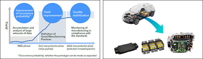 Fig. 3 Contribution to Every Phase of Semiconductor Manufacturing / Fig. 4 Power Modules and Automotive electrical components
By applying our proprietary AI technology, inspection settings have been automated and AI image processing technology for generating high-definition images that facilitate determination of good/defective products has been reinforced. Moreover, the creation of inspection programs for image processing, which was previously reliant on the expertise of experienced technicians, has been automated. This function will help address labor shortages in the semiconductor industry, which are becoming more pressing as a result of technological innovation.
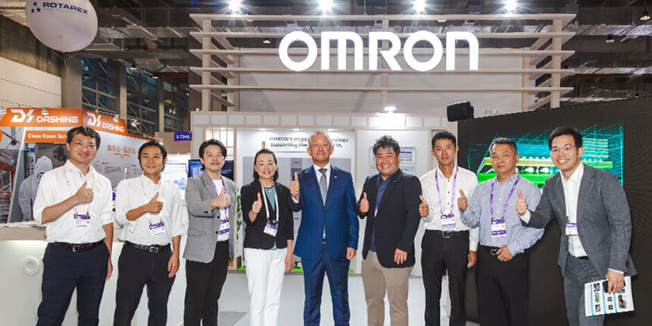
Devices indispensable for an advanced digital society offer higher performance and greater ease of use, but at the same time, their technical structures have become more complex, and from a manufacturing perspective, quality assurance through appearance and functional inspections is becoming more difficult. Going forward, as technological innovation propels semiconductor performance to new heights, advanced inspection technology will remain essential for stable production and high quality. OMRON presented these technologies at SEMICON TAIWAN held from September 4 to September 6, 2024. In Taiwan, a hub of advanced semiconductor manufacturing, we presented our innovation-driven value proposition to numerous customers from the semiconductor industry.
 OMRON's booth at SEMICON TAIWAN
OMRON's offering is by no means limited to PCBA inspection systems, but encompasses many other products and solutions for improving productivity and quality in the semiconductor industry. By continuing to create solutions that underpin technological innovation, we aim to support the digital society, creating a better society and a brighter future.
Figure 1 Semiconductor Industry's Evolution and Challenges
A chiplet is a single package incorporating multiple tiny chips on a substrate, as opposed to a large-scale integrated circuit on a single chip.