Corporate
|
Global
Corporate
|
Global

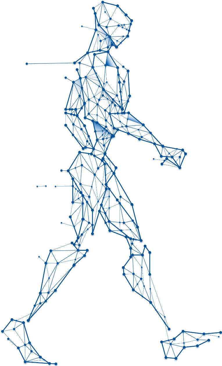

OUR TECHNOLOGY
This is one of the principles that OMRON founder Kazuma Tateishi advocated for as he worked toward innovation driven by social needs, creating the world’s first unmanned railway station system and other innovations based on revolutionary technology.This is the bedrock of OMRON’s R&D strategy as we continue to shape the future.

Based on our core technology that drive the creation of social needs,
we will solve social issues through 5 businesses


News
Apr.3,2026
News
Nov.26,2025
News
Aug.25,2025
News
Jul.11,2025
News
Apr.3,2026
News
Nov.26,2025
News
Aug.25,2025
News
Jul.11,2025
News
Apr.3,2026
News
Nov.26,2025
News
Aug.25,2025
News
Jul.11,2025